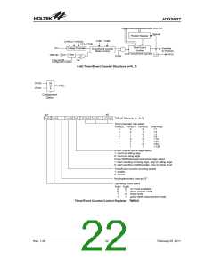
HT45R37
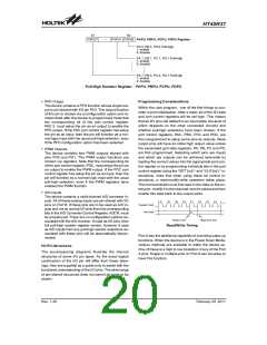
Register - CLKMOD
can be woken up via external switches. Each pin on Port
A can be selected individually to have this wake-up fea-
ture using the PAWU register.
The device operates using a dual clock system whose
mode is controlled using this register. The register con-
trols functions such as the clock source, the idle mode
enable and the division ratio for the slow clock.
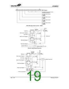
Port A Open Drain Function
All I/O pins in the device have CMOS structures, how-
ever Port A pins PA0~PA3 can also be setup as open
drain structures. This is implemented using the ODE0~
ODE3 bits in the MISC register.
Miscellaneous Register - MISC
The miscellaneous register is used to control two func-
tions. The four lower bits are used for the Watchdog
Timer control, while the highest four bits are used to se-
lect open drain outputs for pins PA0~PA3.
I/O Port Control Registers
Each I/O port has its own control register known as PAC,
PBC, PCC and PDC, to control the input/output configu-
ration. With this control register, each CMOS output or
input with or without pull-high resistor structures can be
reconfigured dynamically under software control. Each
pin of the I/O ports is directly mapped to a bit in its asso-
ciated port control register. For the I/O pin to function as
an input, the corresponding bit of the control register
must be written as a ²1². This will then allow the logic
state of the input pin to be directly read by instructions.
When the corresponding bit of the control register is
written as a ²0², the I/O pin will be setup as a CMOS out-
put. If the pin is currently setup as an output, instructions
can still be used to read the output register. However, it
should be noted that the program will in fact only read
the status of the output data latch and not the actual
logic status of the output pin.
Input/Output Ports
Holtek microcontrollers offer considerable flexibility on
their I/O ports. With the input or output designation of ev-
ery pin fully under user program control, pull-high selec-
tions for all ports and wake-up selections on certain
pins, the user is provided with an I/O structure to meet
the needs of a wide range of application possibilities.
The device provides multiple bidirectional input/output
lines labeled with port names PA, PB, PC and PD.
These I/O ports are mapped to the Data Memory with
specific addresses as shown in the Special Purpose
Data Memory table. All of these I/O ports can be used
for input and output operations. For input operation,
these ports are non-latching, which means the inputs
must be ready at the T2 rising edge of instruction ²MOV
A,[m]², where m denotes the port address. For output
operation, all the data is latched and remains un-
changed until the output latch is rewritten.
Pin-shared Functions
The flexibility of the microcontroller range is greatly en-
hanced by the use of pins that have more than one func-
tion. Limited numbers of pins can force serious design
constraints on designers but by supplying pins with
multi-functions, many of these difficulties can be over-
come. For some pins, the chosen function of the
multi-function I/O pins is set by configuration options
while for others the function is set by application pro-
gram control.
Pull-high Resistors
Many product applications require pull-high resistors for
their switch inputs usually requiring the use of an exter-
nal resistor. To eliminate the need for these external re-
sistors, all I/O pins, when configured as an input have
the capability of being connected to an internal pull-high
resistor. These pull-high resistors are selected using
registers PAPU, PBPU, PCPU and PDPU and are im-
plemented using weak PMOS transistors.
·
External Interrupt Inputs
The external interrupt pins INT0 and INT1 are
pin-shared with I/O pins. For applications not requiring
external interrupt inputs, the pin-shared external inter-
rupt pin can be used as a normal I/O pin, however to
do this, the external interrupt enable bits in the INTC0
register must be disabled.
Port A Wake-up
The HALT instruction forces the microcontroller into a
Power Down condition which preserves power, a fea-
ture that is important for battery and other low-power ap-
plications. Various methods exist to wake-up the
microcontroller, one of which is to change the logic
condition on one of the Port A pins from high to low. After
a HALT instruction forces the microcontroller into enter-
ing a Power Down condition, the processor will remain
in a low-power state until the logic condition of the se-
lected wake-up pin on Port A changes from high to low.
This function is especially suitable for applications that
·
External Timer Clock Input
The external timer pins TMR0 and TMR1 are
pin-shared with I/O pins. To configure them to operate
as timer inputs, the corresponding control bits in the
timer control register must be correctly set and the pin
must also be setup as an input. Note that the original
I/O function will remain even if the pin is setup to be
used as an external timer input.
Rev. 1.20
18
February 25, 2011
图片预览")
 HOLTEK [ HOLTEK SEMICONDUCTOR INC ]