Preliminary
HT45R04/HT45R04E
Data EEPROM Functional Description
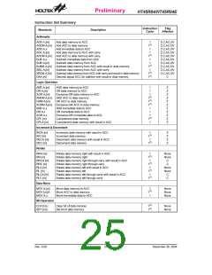
·
Serial clock (SCL)
Device Addressing
The SCL input is used for positive edge clock data into
each EEPROM device and negative edge clock data
out of each device.
The 1K EEPROM devices all require an 8-bit device ad-
dress word following a start condition to enable the chip
for a read or write operation. The device address word
consist of a mandatory one, zero sequence for the first
four most significant bits (refer to the diagram showing
the Device Address). This is common to all the
EEPROM device.
·
Serial data (SDA)
The SDA pin is bidirectional for serial data transfer.
The pin is open-drain driven and may be wired-OR
with any number of other open-drain or open collector
devices.
The next three bits are the fixed to be ²0².
The 8th bit of device address is the read/write operation
select bit. A read operation is initiated if this bit is high
and a write operation is initiated if this bit is low.
Memory Organization
·
1K Serial EEPROM
Internally organized with 128 8-bit words, the 1K re-
quires an 8-bit data word address for random word ad-
dressing.
If the comparison of the device address succeed the
EEPROM will output a zero at ACK bit. If not, the chip will
return to a standby state.
Device Operations
1
0
1
0
0
0
0
R
/
W
·
Clock and data transition
Data transfer may be initiated only when the bus is not
busy. During data transfer, the data line must remain
stable whenever the clock line is high. Changes in
data line while the clock line is high will be interpreted
as a START or STOP condition.
D
e
v
i
c
e
A
d
d
r
e
s
s
Write Operations
·
Byte write
A write operation requires an 8-bit data word address
following the device address word and acknowledg-
ment. Upon receipt of this address, the EEPROM will
again respond with a zero and then clock in the first
8-bit data word. After receiving the 8-bit data word, the
EEPROM will output a zero and the addressing de-
vice, such as a microcontroller, must terminate the
write sequence with a stop condition. At this time the
EEPROM enters an internally-timed write cycle to the
non-volatile memory. All inputs are disabled during
this write cycle and EEPROM will not respond until the
write is completed (refer to Byte write timing).
·
·
Start condition
A high-to-low transition of SDA with SCL high is a start
condition which must precede any other command
(refer to Start and Stop Definition Timing diagram).
Stop condition
A low-to-high transition of SDA with SCL high is a stop
condition. After a read sequence, the stop command
will place the EEPROM in a standby power mode (re-
fer to Start and Stop Definition Timing Diagram).
·
Acknowledge
All addresses and data words are serially transmitted
to and from the EEPROM in 8-bit words. The
EEPROM sends a zero to acknowledge that it has re-
ceived each word. This happens during the ninth clock
cycle.
·
Acknowledge polling
To maximise bus throughput, one technique is to allow
the master to poll for an acknowledge signal after the
start condition and the control byte for a write com-
mand have been sent. If the device is still busy imple-
menting its write cycle, then no ACK will be returned.
The master can send the next read/write command
when the ACK signal has finally been received.
D
a
t
a
a
l
l
o
w
e
d
t
o
c
h
a
n
g
e
S
D
A
S
C
L
S
t
a
r
t
N
o
A
C
K
S
t
o
p
A
a
d
d
r
e
s
s
o
r
c
o
n
d
i
t
i
o
n
c
o
n
d
i
t
i
o
n
c
k
n
o
w
l
e
d
g
e
s
t
a
t
e
v
a
l
i
d
D
e
v
i
c
e
a
d
d
r
e
s
s
W
o
r
d
a
d
d
r
e
s
s
D
A
T
A
S
D
A
S
P
R
/
W
S
t
a
r
t
A
C
K
A
C
K
A
C
K
S
t
o
p
Byte Write Timing
Rev. 0.00
21
December 30, 2004

 HOLTEK [ HOLTEK SEMICONDUCTOR INC ]