HT46R4A
In the following table, D0~D8 is the A/D conversion data
result bits.
Analog to Digital Converter
The need to interface to real world analog signals is a
common requirement for many electronic systems.
However, to properly process these signals using a
microcontroller, they must first be converted into digital
signals by A/D converters. By integrating the A/D con-
version electronic circuitry into the microcontroller, the
need for external components is reduced significantly
with the corresponding follow-on benefits of lower costs
and reduced component space requirements.
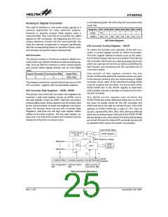
Register Bit7 Bit6 Bit5 Bit4 Bit3 Bit2 Bit1 Bit0
ADRL
ADRH
D0
¾
¾
¾
¾
¾
¾
¾
D8 D7 D6 D5 D4 D3 D2 D1
A/D Data Register
A/D Converter Control Register - ADCR
To control the function and operation of the A/D con-
verter, a control register known as ADCR is provided.
This 8-bit register defines functions such as the selec-
tion of which analog channel is connected to the internal
A/D converter, which pins are used as analog inputs and
which are used as normal I/Os as well as controlling the
start function and monitoring the A/D converter end of
conversion status.
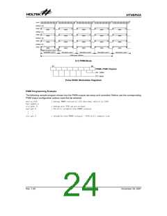
A/D Overview
The device contains a 6-channel analog to digital con-
verter which can directly interface to external analog sig-
nals, such as that from sensors or other control signals
and convert these signals directly into an 9-bit digital
value.
One section of this register contains the bits
ACS2~ACS0 which define the channel number. As each
of the devices contains only one actual analog to digital
converter circuit, each of the individual 6 analog inputs
must be routed to the converter. It is the function of the
ACS2~ACS0 bits in the ADCR register to determine
which analog channel is actually connected to the inter-
nal A/D converter.
Input Channels Conversion Bits
Input Pins
6
9
PB0~PB5
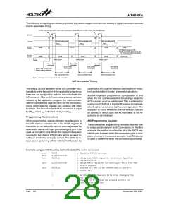
The diagram shows the overall internal structure of the
A/D converter, together with its associated registers.
A/D Converter Data Registers - ADRL, ADRH
The device, has a 9-bit A/D converter, two registers are
required, a high byte register, known as ADRH, and a
low byte register, known as ADRL. After the conversion
process takes place, these registers can be directly read
by the microcontroller to obtain the digitised conversion
value. For devices which use two A/D Converter Data
Registers, note that only the high byte register ADRH
utilises its full 8-bit contents. The low byte register uti-
lises only 1 bit of its 8-bit contents as it contains only the
lowest bit of the 9-bit converted value.
The ADCR control register also contains the
PCR2~PCR0 bits which determine which pins on Port B
are used as analog inputs for the A/D converter and
which pins are to be used as normal I/O pins. If the 3-bit
address on PCR2~PCR0 has a value of ²110², then all
six pins, namely AN0, AN1, AN2, AN3, AN4 and AN5 will
all be set as analog inputs. Note that if the PCR2~PCR0
bits are all set to zero, then all the Port B pins will be setup
as normal I/Os and the internal A/D converter circuitry will
be powered off to reduce the power consumption.
C
l
o
c
k
D
i
v
i
d
e
R
a
t
i
o
C
l
o
c
k
S
o
u
r
c
e
¸
A
C
S
R
R
e
g
i
s
t
e
r
N
S
Y
S
V
D
D
A
/
D
r
e
f
e
r
e
n
c
e
v
o
l
t
a
g
e
P
B
0
/
A
N
0
A
D
R
L
A
D
C
A
D
R
H
P
B
5
/
A
N
5
A
D
C
R
P
C
R
0
~
P
C
R
2
A
D
C
S
0
~
A
D
C
S
2
S
T
A
R
T
E
O
C
B
R
e
g
i
s
t
e
r
P
i
n
C
o
n
f
i
g
u
r
a
t
i
o
n
C
h
a
n
n
e
l
S
e
l
e
c
t
S
t
a
r
t
a
n
d
E
n
d
o
f
B
i
t
s
B
i
t
s
C
o
n
v
e
r
s
i
o
n
B
i
t
s
A/D Converter Structure
Rev. 1.00
25
November 28, 2007

 HOLTEK [ HOLTEK SEMICONDUCTOR INC ]