HT46R4A
Pulse Width Modulator
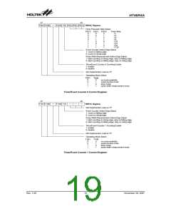
6+2 PWM Mode
Each full PWM cycle, as it is controlled by an 8-bit PWM,
PWM0 or PWM1 register, has 256 clock periods. How-
ever, in the 6+2 PWM Mode, each PWM cycle is subdi-
vided into four individual sub-cycles known as
modulation cycle 0~modulation cycle 3, denoted as ²i²
in the table. Each one of these four sub-cycles contains
64 clock cycles. In this mode, a modulation frequency
increase by a factor of four is achieved. The 8-bit PWM,
PWM0 or PWM1 register value, which represents the
overall duty cycle of the PWM waveform, is divided into
two groups. The first group which consists of bit2~bit7 is
denoted here as the DC value. The second group which
consists of bit0~bit1 is known as the AC value. In the
6+2 PWM mode, the duty cycle value of each of the four
modulation sub-cycles is shown in the following table.
The device contains two Pulse Width Modulation, PWM,
outputs. Useful for such applications such as motor
speed control, the PWM function provides outputs with a
fixed frequency but with a duty cycle that can be varied
by setting particular values into the corresponding PWM
register.
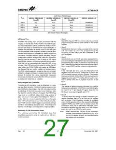
PWM
Mode
Output
Pins
Register
Name
Channels
PD0/
PD1
PWM0/
PWM1
2
6+2
Two registers are provided and are known as PWM0
and PWM1. It is in these registers, that the 8-bit value,
which represents the overall duty cycle of one modula-
tion cycle of the output waveform, should be placed. To
increase the PWM modulation frequency, each modula-
tion cycle is modulated into four individual modulation
sub-sections, known as the 6+2 mode. Note that it is
only necessary to write the required modulation value
into the corresponding PWM register as the subdivision
of the waveform into its sub-modulation cycles is imple-
mented automatically within the microcontroller hard-
ware. For all devices, the PWM clock source is the
DC
Parameter
AC (0~3)
i<AC
(Duty Cycle)
DC+1
64
Modulation cycle i
(i=0~3)
DC
64
i³AC
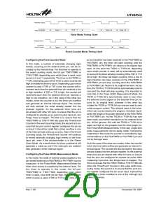
6+2 Mode Modulation Cycle Values
system clock fSYS
.
The diagram illustrates the waveforms associated with
the 6+2 mode of PWM operation. It is important to note
how the single PWM cycle is subdivided into 4 individual
modulation cycles, numbered from 0~3 and how the AC
value is related to the PWM value.
This method of dividing the original modulation cycle
into a further 4 sub-cycles enables the generation of
higher PWM frequencies, which allow a wider range of
applications to be served. As long as the periods of the
generated PWM pulses are less than the time constants
of the load, the PWM output will be suitable as such long
time constant loads will average out the pulses of the
PWM output. The difference between what is known as
the PWM cycle frequency and the PWM modulation fre-
quency should be understood. As the PWM clock is the
system clock, fSYS, and as the PWM value is 8-bits wide,
the overall PWM cycle frequency is fSYS/256, while the
PWM modulation frequency for the 6+2 mode of opera-
tion will be fSYS/64.
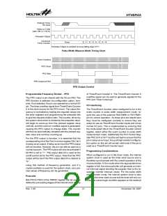
PWM Output Control
The PWM outputs are pin-shared with pins PD0 and
PD1. To operate as PWM outputs and not as I/O pins,
the correct PWM configuration options must be se-
lected. A ²0² must also be written to the corresponding
bit in the I/O port control register, PDC, to ensure that
the required PWM output pin is setup as an output. After
these two initial steps have been carried out, and of
course after the required PWM value has been written
into the PWM register, writing a ²1² to the corresponding
bit in the PD output data register will enable the PWM
data to appear on the pin. Writing a ²0² to the corre-
sponding bit in the PD output data register will disable
the PWM output function and force the output low. In this
way, the Port D data output register can be used as an
on/off control for the PWM function. Note that if the con-
figuration options have selected the PWM function, but
a ²1² has been written to its corresponding bit in the
PDC control register to configure the pin as an input,
then the pin can still function as a normal input line, with
pull-high resistor options.
PWM
PWM Cycle
Frequency
PWM Cycle
Duty
Modulation
Frequency
(PWM register
value)/256
fSYS/64
fSYS/256
Rev. 1.00
23
November 28, 2007

 HOLTEK [ HOLTEK SEMICONDUCTOR INC ]