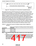
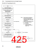
19.3.2 User Programming Mode
When set to user programming mode, the H8/3434F can erase and program its flash memory by
executing a user program. On-board updates of the on-chip flash memory can be carried out by
providing on-board circuits for supplying VPP and data, and storing an update program in part of
the program area.
To select user programming mode, select a mode that enables the on-chip ROM (mode 2 or 3) and
apply 12 V to the FVPP pin, either during a reset, or after the reset has ended (been released) but
while flash memory is not being accessed. In user programming mode, the on-chip supporting
modules operate as they normally would in mode 2 or 3, except for the flash memory. However,
hardware standby mode cannot be set while 12 V is applied to the FVPP pin.
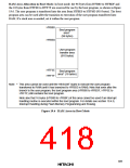
The flash memory cannot be read while it is being programmed or erased, so the update program
must either be stored in external memory, or transferred temporarily to the RAM area and
executed in RAM.
392

 HITACHI [ HITACHI SEMICONDUCTOR ]