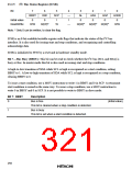
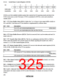
13.2.6 Serial/Timer Control Register (STCR)
Bit
7
6
5
4
3
STAC
0
2
1
ICKS1
0
0
ICKS0
0
IICS
0
IICD
0
IICX
0
IICE
0
MPE
0
Initial value
Read/Write
R/W
R/W
R/W
R/W
R/W
R/W
R/W
R/W
STCR is an 8-bit readable/writable register that controls the SCI operating mode and selects the
TCNT clock source in the 8-bit timers. STCR is initialized to H'00 by a reset and in hardware
standby mode.
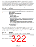
Bit 7—I2C Extra Buffer Select (IICS): Makes bits 7 to 4 of port A into output buffers similar to
SCL and SDA. Used when an I2C bus interface is implemented by software alone.
Bit 7: IICS
Description
0
1
PA7 to PA4 are normal input/output pins
PA7 to PA4 are input/output pins that can drive the bus
(Initial value)
Bit 6—I2C Extra Buffer Reserve (IICD): This bit is reserved, but it can be written and read. Its
initial value is 0.
Bit 5—I2C Transfer Rate Select (IICX): This bit, in combination with bits CKS2 to CKS0 in
ICCR, selects the transfer rate in master mode. For details regarding the transfer rate, refer to
section 13.2.4, I2C Bus Control Register (ICCR).
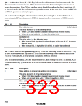
Bit 4—I2C Master Enable (IICE): Controls CPU access to the data and control registers (ICCR,
ICSR, ICDR, ICMR/SAR) of the I2C bus interface.
Bit 4: IICE
Description
0
CPU access to I2C bus interface data and control registers is disabled
(Initial value)
1
CPU access to I2C bus interface data and control registers is enabled
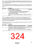
Bit 3—Slave Input Switch (STAC): Switches host interface input pins. For details, see section
14, Host Interface.
Bit 2—Multiprocessor Enable (MPE): Enables or disables the multiprocessor communication
function on channels SCI0 and SCI1. For details, see section 12, Serial Communication Interface.
Bits 1 and 0—Internal Clock Source Select 1 and 0 (ICKS1, ICSK0): These bits select the
clock input to the timer counters (TCNT) in the 8-bit timers. For details, see section 9, 8-Bit
Timers.
296

 HITACHI [ HITACHI SEMICONDUCTOR ]