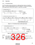
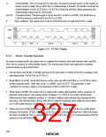
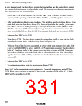
A:
Acknowledge. The receiving device (the slave in master transmit mode, or the master in
master receive mode) drives SDA low to acknowledge a transfer. If transfers need not be
acknowledged, set the ACK bit to 1 in ICCR to keep the interface from generating the
acknowledge signal and its clock pulse.
DATA: Transferred data. The bit length is set by bits BC2 to BC0 in ICMR. The MSB-first or
LSB-first format is selected by bit MLS in ICMR.
P:
Stop condition. The master device drives SDA from low to high while SCL is high.
SDA
SCL
1-7
8
9
1-7
8
9
1-7
8
9
S
SLA
R/W
A
DATA
A
DATA
A/A
P
Figure 13.5 I2C Bus Timing
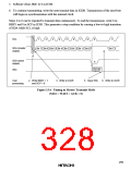
13.3.2 Master Transmit Operation
In master transmit mode, the master device outputs the transmit clock and transmit data, and the
slave device returns an acknowledge signal. The transmit procedure and operations in master
transmit mode are described below.
1. Set bits MLS and WAIT in ICMR and bits ACK and CKS2 to CKS0 in ICCR according to the
operating mode. Set bit ICE in ICCR to 1.
2. Read BBSY in ICSR, check that the bus is free, then set MST and TRS to 1 in ICCR to select
master transmit mode. After that, write 1 in BBSY and 0 in SCP. This generates a start
condition by causing a high-to-low transition of SDA while SCL is high.
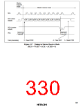
3. Write data in ICDR. The master device outputs the written data together with a sequence of
transmit clock pulses at the timing shown in figure 13.6. If FS is 0 in SAR, the first byte
following the start condition contains a 7-bit slave address and indicates the transmit/receive
direction. The selected slave device (the device with the matching slave address) drives SDA
low at the ninth transmit clock pulse to acknowledge the data.
4. When one byte of data has been transmitted, IRIC is set to 1 in ICSR at the rise of the ninth
transmit clock pulse. If IEIC is set to 1 in ICCR, a CPU interrupt is requested. After one frame
has been transferred, SCL is automatically brought to the low level in synchronization with the
internal clock and held low.
298

 HITACHI [ HITACHI SEMICONDUCTOR ]