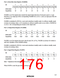
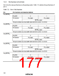
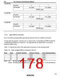
7.12
Port B
7.12.1 Overview
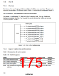
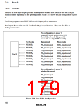
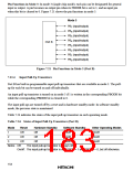
Port B is an 8-bit input/output port that is multiplexed with the host interface data bus. The pin
functions differ depending on the operating mode. Figure 7.19 shows the pin configuration of port
B.
Port B has program-controllable built-in MOS input pull-up transistors.
Pins in port B can drive one TTL load and a 90-pF capacitive load. They can also drive a
darlington transistor.
Pin configuration in mode 1
(expanded mode with on-chip ROM
disabled) and mode 2 (expanded
mode with on-chip ROM enabled)
Port B pins
PB7/XDB7
PB6/XDB6
PB5/XDB5
PB4/XDB4
PB3/XDB3
PB2/XDB2
PB1/XDB1
PB0/XDB0
Master mode
Slave mode
PB7 (input/output)
PB6 (input/output)
PB5 (input/output)
PB4 (input/output)
PB3 (input/output)
PB2 (input/output)
PB1 (input/output)
PB0 (input/output)
XDB7 (input/output)
XDB6 (input/output)
XDB5 (input/output)
XDB4 (input/output)
XDB3 (input/output)
XDB2 (input/output)
XDB1 (input/output)
XDB0 (input/output)
Port B
Pin configuration in mode 3
(single-chip mode)
PB7 (input/output)
PB6 (input/output)
PB5 (input/output)
PB4 (input/output)
PB3 (input/output)
PB2 (input/output)
PB1 (input/output)
PB0 (input/output)
Figure 7.19 Port B Pin Configuration
150

 HITACHI [ HITACHI SEMICONDUCTOR ]