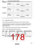
7.12.3 Pin Functions in Each Mode
Port B has different pin functions in different modes. A separate description for each mode is
given below.
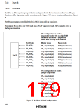
Pin Functions in Modes 1 and 2: In mode 1 (expanded mode with on-chip ROM disabled) and
mode 2 (expanded mode with on-chip ROM enabled), when the host interface enable bit (HIE) is
cleared to 0 in the system control register (SYSCR), port B is a general-purpose input/output port.
When the HIE bit is set to 1, selecting slave mode, port B becomes the host interface data bus
(XDB7 to XDB0). PBODR and PBDDR should be cleared to H'00 in slave mode. For details, see
section 14, Host Interface.
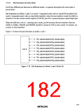
Figure 7.20 shows the pin functions in modes 1 and 2.
PB7 (input/output)/XDB7 (input/output)
PB6 (input/output)/XDB6 (input/output)
PB5 (input/output)/XDB5 (input/output)
PB4 (input/output)/XDB4 (input/output)
Port B
PB3 (input/output)/XDB3 (input/output)
PB2 (input/output)/XDB2 (input/output)
PB1 (input/output)/XDB1 (input/output)
PB0 (input/output)/XDB0 (input/output)
Figure 7.20 Pin Functions in Modes 1 and 2 (Port B)
153

 HITACHI [ HITACHI SEMICONDUCTOR ]