7.11
Port A
7.11.1 Overview
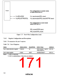
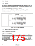
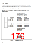
Port A is an 8-bit input/output port that is multiplexed with key-sense input pins. The port A pin
functions are the same in all operating modes. Figure 7.18 shows the pin configuration of port A.
Port A has built-in, programming MOS input pull-up transistors.
Pins in port A can drive one TTL load and a 90-pF capacitive load. They can also drive a
darlington transistor. Pins PA4, PA5, PA6, and PA7 can be driven as bus buffers, as shown in
section 13, I2C Bus Interface.
Port A pins
PA7 (input/output)/KEYIN15 (input)
PA6 (input/output)/KEYIN14 (input)
PA5 (input/output)/KEYIN13 (input)
PA4 (input/output)/KEYIN12 (input)
Port A
PA3 (input/output)/KEYIN11 (input)
PA2 (input/output)/KEYIN10 (input)
PA1 (input/output)/KEYIN9 (input)
PA0 (input/output)/KEYIN8 (input)
Figure 7.18 Port A Pin Configuration
7.11.2 Register Configuration and Descriptions
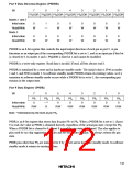
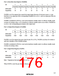
Table 7.20 summarizes the port A registers.
Table 7.20 Port A Registers
Name
Abbreviation
PADDR
Read/Write
Initial Value
H'00
Address
H'FFAB
H'FFAA
Port A data direction register
Port A output data register
Port A input data register
W
PAODR
R/W
R
H'00
PAPIN
Undetermined H'FFAB
Note: The data direction register (PADDR) and input data register (PAPIN) have the same
address.
146

 HITACHI [ HITACHI SEMICONDUCTOR ]