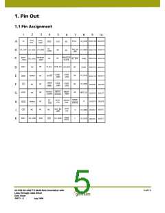
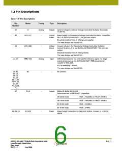
1.2 Pin Descriptions
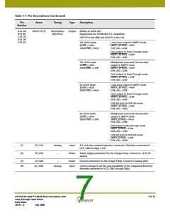
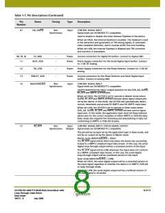
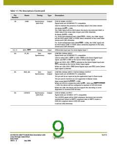
Table 1-1: Pin Descriptions
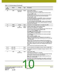
Pin
Name
Timing
Type
Description
Number
A1
LF
Analog
–
Output
Control voltage to external Voltage Controlled Oscillator. Nominally
+1.25V DC.
A2
VCO_VCC
Output
Power
Power Supply for the external Voltage Controlled Oscillator. Connect to
pin 7 of the GO1555/GO1525*. This pin is an output.
Should be isolated from all other power supplies.
*For new designs use the GO1555.
A3
VCO_GND
VCO, VCO
NC
–
Analog
–
Output
Power
Ground reference for the external Voltage Controlled Oscillator.
Connect to pins 2, 4, 6, and 8 of the GO1555/GO1525*. This pin is an
output.
Should be isolated from all other grounds.
*For new designs use the GO1555.
A4, A5
Input
Differential inputs for the external VCO reference signal. For single
ended devices such as the GO1555/GO1525*, VCO should be AC
coupled to VCO_GND.
VCO is nominally 1.485GHz.
*For new designs use the GO1555.
A6, B5,
B6, C4,
–
No Connect.
C5, D2,
D3, D7,
E3, E7, F2,
F3, F7, G2,
G3, G7,
H3, J2, J3,
J4,
A7
PCLK
–
Output
PARALLEL DATA BUS CLOCK
Signal levels are LVCMOS/LVTTL compatible.
HD 20-bit mode
HD 10-bit mode
SD 20-bit mode
SD 10-bit mode
PCLK = 74.25MHz or 74.25/1.001MHz
PCLK = 148.5MHz or 148.5/1.001MHz
PCLK = 13.5MHz
PCLK = 27MHz
A8, E8, K8
IO_VDD
–
Power
Power Supply connection for digital I/O buffers. Connect to +3.3V DC
digital.
GS1559 HD-LINX™ II Multi-Rate Deserializer with
Loop-Through Cable Driver
Data Sheet
6 of 71
30572 - 8
July 2008

 GENNUM [ GENNUM CORPORATION ]