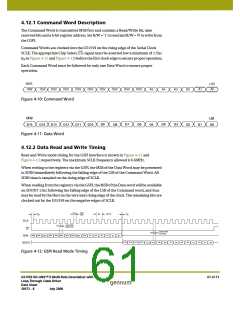
duty
cycle
period
t2
t
4
t0
SCLK
input data
setup time
t
3
CS
RSV
R/W
RSV
RSV
RSV RSV
RSV
RSV
A5
A4
A3
A2
D9
SDIN
RSV
A1
A0
D15 D14
D13
D12
D7
D5
D4
D2
RSV
D10
D8
D6
D3
D1
D0
D11
Figure 4-13: GSPI Write Mode Timing
4.12.3 Configuration and Status Registers
Table 4-17 summarizes the GS1559's internal status and configuration registers.
All of these registers are available to the Host via the GSPI and are all individually
addressable.
Where status registers contain less than the full 16 bits of information however, two or
more registers may be combined at a single logical address.
Table 4-17: GS1559 internal registers
Address
Register Name
See Section
000h
IOPROC_DISABLE
ERROR_STATUS
EDH_FLAG
Section 4.10.6
Section 4.10.5
Section 4.10.7
Section 4.10.4
Section 4.10.2.1
Section 4.10.3
Section 4.10.4
Section 4.10.5.2
Section 4.10.5
001h
003h
004h
VIDEO_STANDARD
ANC_TYPE
005h - 009h
00Ch - 00Dh
00Eh - 011h
012h - 019h
01Ah
VIDEO_FORMAT
RASTER_STRUCTURE
EDH_CALC_RANGES
ERROR_MASK
GS1559 HD-LINX™ II Multi-Rate Deserializer with
Loop-Through Cable Driver
Data Sheet
62 of 71
30572 - 8
July 2008

 GENNUM [ GENNUM CORPORATION ]