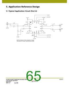
4.12.1 Command Word Description
The Command Word is transmitted MSB first and contains a Read/Write bit, nine
reserved bits and a 6-bit register address. Set R/W = '1' to read and R/W = '0' to write from
the GSPI.
Command Words are clocked into the GS1559 on the rising edge of the Serial Clock
SCLK. The appropriate Chip Select, CS, signal must be asserted low a minimum of 1.5ns
(t in Figure 4-12 and Figure 4-13) before the first clock edge to ensure proper operation.
0
Each Command Word must be followed by only one Data Word to ensure proper
operation.
MSB
LSB
A0
R/W
RSV
RSV
RSV
RSV
RSV
RSV
RSV
RSV
RSV
A5
A4
A3
A2
A1
Figure 4-10: Command Word
MSB
LSB
D9
D7
D6
D4
D3
D15
D14
D13
D12
D11
D10
D8
D5
D2
D1
D0
Figure 4-11: Data Word
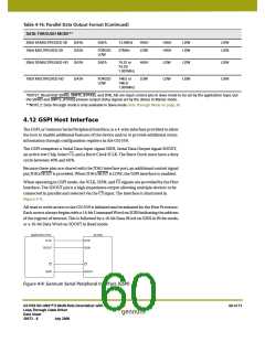
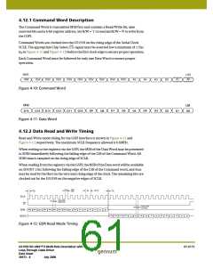
4.12.2 Data Read and Write Timing
Read and Write mode timing for the GSPI interface is shown in Figure 4-12 and
Figure 4-13 respectively. The maximum SCLK frequency allowed is 6.6MHz.
When writing to the registers via the GSPI, the MSB of the Data Word may be presented
to SDIN immediately following the falling edge of the LSB of the Command Word. All
SDIN data is sampled on the rising edge of SCLK.
When reading from the registers via the GSPI, the MSB of the Data word will be available
on SDOUT 12ns following the falling edge of the LSB of the Command word, and thus
may be read by the Host on the very next rising edge of the clock. The remaining bits are
clocked out by the GS1559 on the negative edges of SCLK.
duty
cycle
period
t
2
t4
t0
t5
SCLK
input data
setup time
t3
CS
SDIN
output data
hold time
t6
RSV
R/W
RSV
RSV
RSV RSV
RSV
RSV
A5
A4
A3
A2
RSV
RSV
A1
A0
D9
D15 D14
D13
D12
D7
D5
D4
D2
D10
D8
D6
D3
D1
D0
D11
SDOUT
Figure 4-12: GSPI Read Mode Timing
GS1559 HD-LINX™ II Multi-Rate Deserializer with
Loop-Through Cable Driver
Data Sheet
61 of 71
30572 - 8
July 2008

 GENNUM [ GENNUM CORPORATION ]