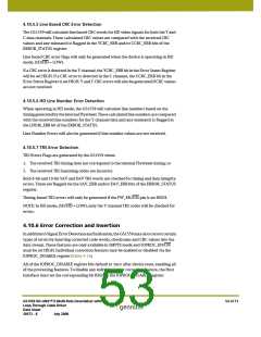
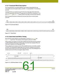
4.11 Parallel Data Outputs
Data outputs leave the device on the rising edge of PCLK as shown in Figure 4-7 and
Figure 4-8.
The data may be scrambled or unscrambled, framed or unframed, and may be presented
in 10-bit or 20-bit format. The output data bus width is controlled independently from
the internal data bus width by the 20bit/10bit input pin.
Likewise, the output data format is defined by the setting of the external SD/HD,
SMPTE_BYPASS and DVB_ASI pins. Recall that in Slave mode, these pins are set by the
application layer as inputs to the device. In Master mode, however, the GS1559 sets the
SD/HD and SMPTE_BYPASS pins as output status signals.
4.11.1 Parallel Data Bus Buffers
The parallel data outputs of the GS1559 are driven by high-impedance buffers which
support both LVTTL and LVCMOS levels. These buffers use a separate power supply of
+3.3V DC supplied via the IO_VDD and IO_GND pins.
All output buffers, including the PCLK output, may be driven to a high-impedance state
if the RESET_TRST signal is asserted LOW.
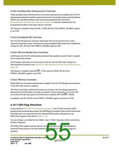
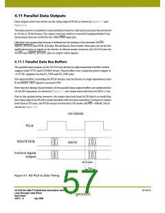
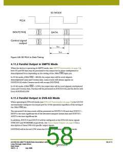
Note that the timing characteristics of the parallel data output buffers are optimized for
10-bit HD operation. As shown in Figure 4-7, the output data hold time for HD is 1.5ns.
Due to this optimization, however, the output data hold time for SD data is so small that
the rising edge of the PCLK is nearly incident with the data transition. To improve output
hold time at SD rates, the PCLK output is inverted is SD mode, (SD/HD = HIGH). This is
shown in Figure 4-8.
HD MODE
PCLK
DOUT[19:0]
DATA
Control signal
output
tOH
tOD
Figure 4-7: HD PCLK to Data Timing
GS1559 HD-LINX™ II Multi-Rate Deserializer with
Loop-Through Cable Driver
Data Sheet
57 of 71
30572 - 8
July 2008

 GENNUM [ GENNUM CORPORATION ]