Contents
Key Features........................................................................................................................................................1
Applications.........................................................................................................................................................1
Description...........................................................................................................................................................1
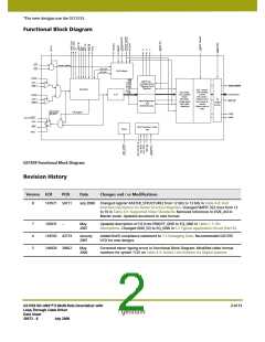
Functional Block Diagram ..............................................................................................................................2
Revision History .................................................................................................................................................2
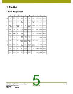
1. Pin Out..............................................................................................................................................................5
1.1 Pin Assignment..................................................................................................................................5
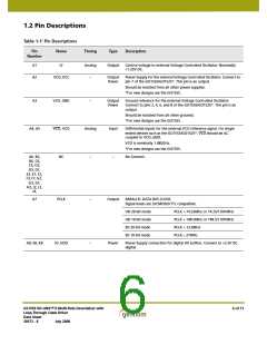
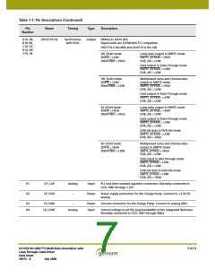
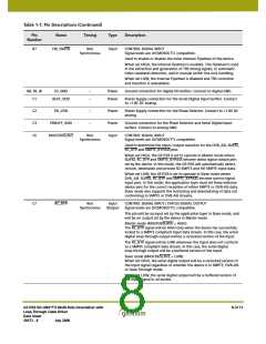
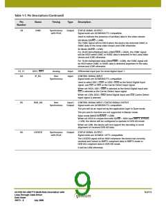
1.2 Pin Descriptions ................................................................................................................................6
2. Electrical Characteristics ........................................................................................................................ 16
2.1 Absolute Maximum Ratings....................................................................................................... 16
2.2 DC Electrical Characteristics ..................................................................................................... 16
2.3 AC Electrical Characteristics ..................................................................................................... 18
3. Input/Output Circuits .............................................................................................................................. 20
3.1 Host Interface Map........................................................................................................................ 22
3.1.1 Host Interface Map (R/W Configurable Registers) ................................................ 23
3.1.2 Host Interface Map (Read Only Registers) ............................................................... 24
4. Detailed Description................................................................................................................................. 25
4.1 Functional Overview.................................................................................................................... 25
4.2 Serial Digital Input ........................................................................................................................ 25
4.2.1 Input Signal Selection ..................................................................................................... 25
4.2.2 Carrier Detect Input......................................................................................................... 26
4.2.3 Single Input Configuration............................................................................................ 26
4.3 Serial Digital Reclocker ............................................................................................................... 26
4.3.1 External VCO..................................................................................................................... 26
4.3.2 Loop Bandwidth................................................................................................................ 27
4.4 Serial Digital Loop-Through Output........................................................................................ 27
4.4.1 Output Swing..................................................................................................................... 27
4.4.2 Reclocker Bypass Control.............................................................................................. 28
4.4.3 Serial Digital Output Mute............................................................................................. 28
4.5 Serial-To-Parallel Conversion ................................................................................................... 29
4.6 Modes Of Operation ..................................................................................................................... 29
4.6.1 Lock Detect ......................................................................................................................... 29
4.6.2 Master Mode....................................................................................................................... 30
4.6.3 Slave Mode.......................................................................................................................... 31
4.7 SMPTE Functionality .................................................................................................................... 31
4.7.1 SMPTE Descrambling and Word Alignment ........................................................... 32
4.7.2 Internal Flywheel ............................................................................................................. 32
4.7.3 Switch Line Lock Handling............................................................................................ 33
4.7.4 HVF Timing Signal Generation .................................................................................... 36
4.8 DVB-ASI Functionality ................................................................................................................ 38
4.8.1 DVB-ASI 8b/10b Decoding and Word Alignment................................................. 38
4.8.2 Status Signal Outputs ...................................................................................................... 38
GS1559 HD-LINX™ II Multi-Rate Deserializer with
Loop-Through Cable Driver
Data Sheet
3 of 71
30572 - 8
July 2008

 GENNUM [ GENNUM CORPORATION ]