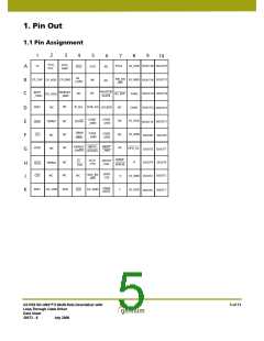
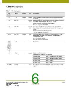
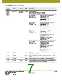
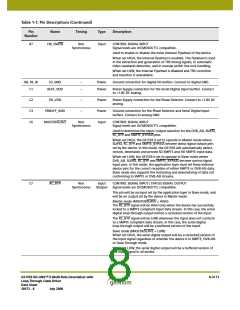
*For new designs use the GO1555.
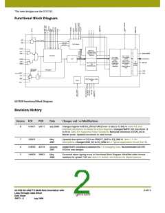
Functional Block Diagram
CD1
CD2
carrier_detect
rclk_ctrl
pll_lock
LOCK detect
TERM 1
SMPTE De-
scramble, Word
alignment and
flywheel
DDI_1
DDI_1
DATA_ERROR
Reclocker
CRC correct
Line number
correct
TRS correct
CSUM correct
EDH check &
correct
CRC check
Line number
check
TRS check
CSUM check
ANC data
detection
S->P
DOUT[19:0]
FIFO_LD
TERM 2
DDI_2
DDI_2
I/O
Word alignment
and
8b/10b decode
Buffer
& mux
Illegal code re-
map
(o/p mute)
pll_lock
rclk_bypass
CANC
YANC
SDO_EN/DIS
SDO
SDO
HOST Interface / JTAG
Reset
test
RSET
GS1559 Functional Block Diagram
Revision History
Version ECR
PCN
Date
Changes and / or Modifications
8
147971
50711
July 2008
Changed register RASTER_STRUCTURE2 from 12 bits to 13 bits in Table 4-8: Host
Interface Description for Raster Structure Registers. Changed SMPTE 352 Lines from 13
to 10 in Table 4-9: Supported Video Standards. Removed references to DVB_ASI in
Master mode. Updated document to new format.
7
6
5
145031
143592
140420
–
May
2007
Updated description of H2 from PDBUFF_GND to EQ_GND in Table 1-1: Pin
Descriptions. Changed GND_EQ to EQ_GND in 5.2 Typical Application Circuit (Part B).
42774
39452
January
2007
Added RoHS compliance statement to 7.3 Packaging Data. Recommended GO1555
VCO for new designs.
May
2006
Corrected minor typing errors in Functional Block Diagram. Modified video format
numbers for system 1125 on Table 4-4: Switch Line Position for Digital Systems.
GS1559 HD-LINX™ II Multi-Rate Deserializer with
Loop-Through Cable Driver
Data Sheet
2 of 71
30572 - 8
July 2008

 GENNUM [ GENNUM CORPORATION ]