Document Revision History
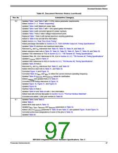
Table 61. Document Revision History (continued)
Substantive Change(s)
Rev. No.
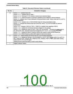
2.0
Section 1.1—Updated features list to coincide with latest version of the reference manual
Table 1 and Table 2—Addition of SYSCLK to OVIN
Table 2—Addition of notes 1 and 2
Table 3—Addition of note 1
Table 5—New
Section 4—New
Table 13—Addition of IVREF
Removed Figure 4 DDR SRAM Input TIming Diagram
Table 15—Modified maximum values for tDISKEW
Table 16—Added MSYNC_OUT to tMCKSKEW2
Figure 4—New
Section 6.2.1—Removed Figure 4, “DDR SDRAM Input Timing Diagram”
Section 8.1—Removed references to 2.5 V from first paragraph
Figure 7—New
Table 21 and Table 22—Modified “conditions” for IIH and I IL
Table 23—Addition of min and max for GTX_CLK125 reference clock duty cycle
Table 27 —Addition of min and max for GTX_CLK125 reference clock duty cycle
Table 29—Addition of min and max for GTX_CLK125 reference clock duty cycle
Table 30—VOH min and conditions; IIH and I IL conditions
Table 31—Min and max for tMTXR and tMTXF
Table 32—Min and max for tMRXR and tMRXF
Figure 22 and Figure 23—Changed LSYNC_IN to Internal clock at top of each figure
Figure 17—New
Figure 17—New
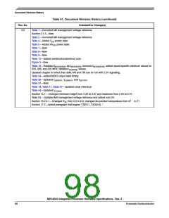
Table 36—Removed row for tLBKHOX3
Table 43—New (AC timing of PCI-X at 66 MHz)
Table 53—Addition of note 19
Figure 54—Addition of jumper and note at top of diagram
Table 55: Changed max bus freq for 667 core to 166
Section 16.2.1—Modified first paragraph
Figure 45—Modified
Figure 46—New
Table 59—Modified thermal resistance data
Section 16.2.4.2—Modified first and second paragraphs
MPC8540 Integrated Processor Hardware Specifications, Rev. 4
Freescale Semiconductor
99

 FREESCALE [ Freescale ]