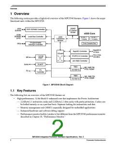
Overview
•
256 Kbyte L2 cache/SRAM
— Can be configured as follows
– Full cache mode (256-Kbyte cache).
– Full memory-mapped SRAM mode (256-Kbyte SRAM mapped as a single 256-Kbyte
block or two 128-Kbyte blocks)
– Half SRAM and half cache mode (128-Kbyte cache and 128-Kbyte memory-mapped
SRAM)
— Full ECC support on 64-bit boundary in both cache and SRAM modes
— Cache mode supports instruction caching, data caching, or both
— External masters can force data to be allocated into the cache through programmed memory
ranges or special transaction types (stashing)
— Eight-way set-associative cache organization (1024 sets of 32-byte cache lines)
— Supports locking the entire cache or selected lines. Individual line locks are set and cleared
through Book E instructions or by externally mastered transactions
— Global locking and flash clearing done through writes to L2 configuration registers
— Instruction and data locks can be flash cleared separately
— Read and write buffering for internal bus accesses
— SRAM features include the following:
– I/O devices access SRAM regions by marking transactions as snoopable (global)
– Regions can reside at any aligned location in the memory map
– Byte accessible ECC is protected using read-modify-write transactions accesses for smaller
than cache-line accesses.
•
•
Address translation and mapping unit (ATMU)
— Eight local access windows define mapping within local 32-bit address space
— Inbound and outbound ATMUs map to larger external address spaces
– Three inbound windows plus a configuration window on PCI/PCI-X
– Four inbound windows plus a default and configuration window on RapidIO
– Four outbound windows plus default translation for PCI
– Eight outbound windows plus default translation for RapidIO
DDR memory controller
— Programmable timing supporting DDR-1 SDRAM
— 64-bit data interface, up to 333-MHz data rate
— Four banks of memory supported, each up to 1 Gbyte
— DRAM chip configurations from 64 Mbits to 1 Gbit with x8/x16 data ports
— Full ECC support
— Page mode support (up to 16 simultaneous open pages)
— Contiguous or discontiguous memory mapping
MPC8540 Integrated Processor Hardware Specifications, Rev. 4
Freescale Semiconductor
3

 FREESCALE [ Freescale ]