Electrical Characteristics
2.1.2 Power Sequencing
The MPC8540 requires its power rails to be applied in a specific sequence in order to ensure proper device
operation. These requirements are as follows for power up:
1. V , AV
DD
DD
2. GV , LV , OV (I/O supplies)
DD
DD
DD
Items on the same line have no ordering requirement with respect to one another. Items on separate lines
must be ordered sequentially such that voltage rails on a previous step must reach 90 percent of their value
before the voltage rails on the current step reach 10 percent of theirs.
NOTE
If the items on line 2 must precede items on line 1, please ensure that the
delay will not exceed 500 ms and the power sequence is not done greater
than once per day in production environment.
NOTE
From a system standpoint, if the I/O power supplies ramp prior to the VDD
core supply, the I/Os on the MPC8540 may drive a logic one or zero during
power-up.
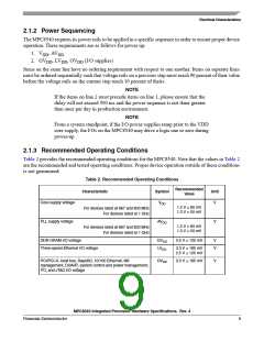
2.1.3 Recommended Operating Conditions
Table 2 provides the recommended operating conditions for the MPC8540. Note that the values in Table 2
are the recommended and tested operating conditions. Proper device operation outside of these conditions
is not guaranteed.
Table 2. Recommended Operating Conditions
Recommended
Characteristic
Symbol
Unit
Value
Core supply voltage
PLL supply voltage
DDR DRAM I/O voltage
VDD
V
1.2 V 60 mV
1.3 V 50 mV
For devices rated at 667 and 833 MHz
For devices rated at 1 GHz
AVDD
V
1.2 V 60 mV
1.3 V 50 mV
For devices rated at 667 and 833 MHz
For devices rated at 1 GHz
GVDD
LVDD
2.5 V 125 mV
V
V
Three-speed Ethernet I/O voltage
3.3 V 165 mV
2.5 V 125 mV
PCI/PCI-X, local bus, RapidIO, 10/100 Ethernet, MII
management, DUART, system control and power management,
I2C, and JTAG I/O voltage
OVDD
3.3 V 165 mV
V
MPC8540 Integrated Processor Hardware Specifications, Rev. 4
Freescale Semiconductor
9

 FREESCALE [ Freescale ]