Electrical Characteristics
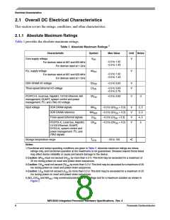
2.1 Overall DC Electrical Characteristics
This section covers the ratings, conditions, and other characteristics.
2.1.1 Absolute Maximum Ratings
Table 1 provides the absolute maximum ratings.
1
Table 1. Absolute Maximum Ratings
Characteristic
Core supply voltage
Symbol
Max Value
Unit Notes
VDD
V
–0.3 to 1.32
–0.3 to 1.43
For devices rated at 667 and 833 MHz
For devices rated at 1 GHz
PLL supply voltage
AVDD
V
–0.3 to 1.32
–0.3 to 1.43
For devices rated at 667 and 833 MHz
For devices rated at 1 GHz
DDR DRAM I/O voltage
GVDD
LVDD
–0.3 to 3.63
V
V
Three-speed Ethernet I/O voltage
–0.3 to 3.63
–0.3 to 2.75
PCI/PCI-X, local bus, RapidIO, 10/100 Ethernet, MII
management, DUART, system control and power
management, I2C, and JTAG I/O voltage
OVDD
–0.3 to 3.63
V
3
Input voltage
DDR DRAM signals
MVIN
MVREF
LVIN
–0.3 to (GVDD + 0.3)
–0.3 to (GVDD + 0.3)
–0.3 to (LVDD + 0.3)
–0.3 to (OVDD + 0.3)
V
V
V
V
2, 5
2, 5
4, 5
5
DDR DRAM reference
Three-speed Ethernet signals
PCI/PCI-X, Local bus, RapidIO,
10/100 Ethernet, DUART,
SYSCLK, system control and
power management, I2C, and
JTAG signals
OVIN
Storage temperature range
TSTG
–55 to 150
•C
Notes:
1.Functional and tested operating conditions are given in Table 2. Absolute maximum ratings are stress
ratings only, and functional operation at the maximums is not guaranteed. Stresses beyond those listed
may affect device reliability or cause permanent damage to the device.
2.Caution: MVIN must not exceed GVDD by more than 0.3 V. This limit may be exceeded for a maximum of
20 ms during power-on reset and power-down sequences.
3.Caution: OVIN must not exceed OVDD by more than 0.3 V. This limit may be exceeded for a maximum of 20
ms during power-on reset and power-down sequences.
4.Caution: LVIN must not exceed LVDD by more than 0.3 V. This limit may be exceeded for a maximum of 20
ms during power-on reset and power-down sequences.
5.(M,L,O)VIN and MVREF may overshoot/undershoot to a voltage and for a maximum duration as shown in
Figure 2.
MPC8540 Integrated Processor Hardware Specifications, Rev. 4
8
Freescale Semiconductor

 FREESCALE [ Freescale ]