Clock Timing
4 Clock Timing
4.1 System Clock Timing
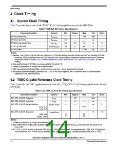
Table 7 provides the system clock (SYSCLK) AC timing specifications for the MPC8540.
Table 7. SYSCLK AC Timing Specifications
Parameter/Condition
SYSCLK frequency
Symbol
Min
Typical
Max
Unit
Notes
fSYSCLK
tSYSCLK
KH, tKL
tKHKL/tSYSCLK
—
—
6.0
0.6
40
—
—
—
166
—
MHz
ns
1
SYSCLK cycle time
SYSCLK rise and fall time
SYSCLK duty cycle
SYSCLK jitter
t
1.0
—
1.2
ns
2
3
60
%
—
+/- 150
ps
4, 5
Notes:
1.Caution: The CCB to SYSCLK ratio and e500 core to CCB ratio settings must be chosen such that the resulting SYSCLK
frequency, e500 (core) frequency, and CCB frequency do not exceed their respective maximum or minimum operating
frequencies. Refer to Section 15.2, “Platform/System PLL Ratio,” and Section 15.3, “e500 Core PLL Ratio,” for ratio
settings.
2. Rise and fall times for SYSCLK are measured at 0.6 V and 2.7 V.
3. Timing is guaranteed by design and characterization.
4. This represents the total input jitter—short term and long term—and is guaranteed by design.
5. For spread spectrum clocking, guidelines are +/-1% of the input frequency with a maximum of 60 kHz of modulation
regardless of the input frequency.
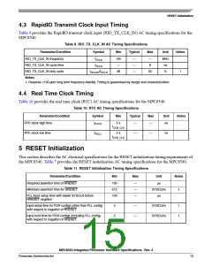
4.2 TSEC Gigabit Reference Clock Timing
Table 7 provides the TSEC gigabit reference clock (EC_GTX_CLK125) AC timing specifications for the
MPC8540.
Table 8. EC_GTX_CLK125 AC Timing Specifications
Parameter/Condition
Symbol
Min
Typical
Max
Unit
Notes
EC_GTX_CLK125 frequency
EC_GTX_CLK125 cycle time
EC_GTX_CLK125 rise and fall time
fG125
tG125
—
—
—
125
8
—
—
MHz
ns
t
G125R, tG125F
—
ns
2
0.75
1
LVDD=2.5
LVDD=3.3
EC_GTX_CLK125 duty cycle
tG125H/tG125
—
%
1,3
45
47
55
53
GMII, TBI
RGMII, RTBI
Notes:
1. Timing is guaranteed by design and characterization.
2. Rise and fall times for EC_GTX_CLK125 are measured from 0.5V and 2.0V for LVDD=2.5V, and from 0.6 and 2.7V for
LVDD=3.3V.
3. EC_GTX_CLK125 is used to generate GTX clock for TSEC transmitter with 2% degradation EC_GTX_CLK125 duty cycle
can be loosened from 47/53% as long as PHY device can tolerate the duty cycle generated by GTX_CLK of TSEC.
MPC8540 Integrated Processor Hardware Specifications, Rev. 4
14
Freescale Semiconductor

 FREESCALE [ Freescale ]