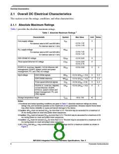
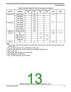
Power Characteristics
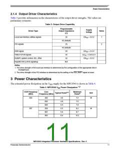
2.1.4 Output Driver Characteristics
Table 3 provides information on the characteristics of the output driver strengths. The values are
preliminary estimates.
Table 3. Output Drive Capability
Programmable
Supply
Driver Type
Output Impedance
Notes
Voltage
(Ω)
Local bus interface utilities signals
25
OVDD = 3.3 V
1
42 (default)
PCI signals
25
2
42 (default)
DDR signal
20
42
GVDD = 2.5 V
LVDD = 2.5/3.3 V
OVDD = 3.3 V
TSEC/10/100 signals
DUART, system control, I2C, JTAG
RapidIO N/A (LVDS signaling)
Notes:
42
N/A
1. The drive strength of the local bus interface is determined by the configuration of the appropriate bits in
PORIMPSCR.
2. The drive strength of the PCI interface is determined by the setting of the PCI_GNT1 signal at reset.
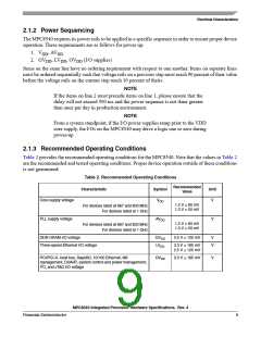
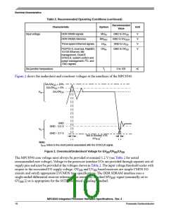
3 Power Characteristics
The estimated power dissipation on the V supply for the MPC8540 is shown in Table 4.
DD
1,2
Table 4. MPC8540 V Power Dissipation
DD
CCB Frequency
(MHz)
Core
Frequency (MHz)
Maximum
Typical Power3,4
Unit
Power5
200
400
500
600
533
667
800
4.6
4.9
5.3
5.5
5.9
6.4
7.2
7.5
W
7.9
267
8.2
W
8.7
10.2
MPC8540 Integrated Processor Hardware Specifications, Rev. 4
Freescale Semiconductor
11

 FREESCALE [ Freescale ]