Electrical Characteristics
Table 2. Recommended Operating Conditions (continued)
Recommended
Value
Characteristic
DDR DRAM signals
Symbol
Unit
Input voltage
MVIN
MVREF
LVIN
GND to GVDD
GND to GVDD/2
GND to LVDD
GND to OVDD
V
V
V
V
DDR DRAM reference
Three-speed Ethernet signals
PCI/PCI-X, local bus, RapidIO,
10/100 Ethernet, MII
OVIN
management, DUART,
SYSCLK, system control and
power management, I2C, and
JTAG signals
Die-junction temperature
Tj
0 to 105
•C
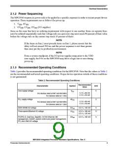
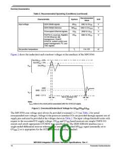
Figure 2 shows the undershoot and overshoot voltages at the interfaces of the MPC8540.
G/L/OVDD + 20%
G/L/OVDD + 5%
G/L/OVDD
VIH
GND
GND – 0.3 V
VIL
GND – 0.7 V
Not to Exceed 10%
1
of tSYS
Note:
tSYS refers to the clock period associated with the SYSCLK signal.
Figure 2. Overshoot/Undershoot Voltage for GV /OV /LV
DD
DD
DD
The MPC8540 core voltage must always be provided at nominal 1.2 V (see Table 2 for actual
recommended core voltage). Voltage to the processor interface I/Os are provided through separate sets of
supply pins and must be provided at the voltages shown in Table 2. The input voltage threshold scales with
respect to the associated I/O supply voltage. OV and LV based receivers are simple CMOS I/O
DD
DD
circuits and satisfy appropriate LVCMOS type specifications. The DDR SDRAM interface uses a
single-ended differential receiver referenced the externally supplied MV signal (nominally set to
REF
GV /2) as is appropriate for the SSTL2 electrical signaling standard.
DD
MPC8540 Integrated Processor Hardware Specifications, Rev. 4
10
Freescale Semiconductor

 FREESCALE [ Freescale ]