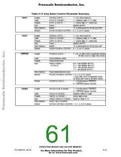
Freescale Semiconductor, Inc.
Semiconductor wafer processing causes variations of the RC time-out values between
individual devices. An E-clock frequency below 10 kHz is detected as a clock monitor
error. An E-clock frequency of 200 kHz or more prevents clock monitor errors. Using
the clock monitor function when the E-clock is below 200 kHz is not recommended.
Special considerations are needed when a STOP instruction is executed and the clock
monitor is enabled. Because the STOP function causes the clocks to be halted, the
clock monitor function generates a reset sequence if it is enabled at the time the STOP
mode was initiated. Before executing a STOP instruction, clear to zero the CME bit in
the OPTION register to disable the clock monitor. After recovery from STOP, set the
CME bit to logic one to enable the clock monitor.
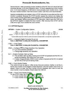
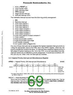
5.1.5 OPTION Register
OPTION — System Configuration Options
$1039
Bit 7
ADPU
0
6
CSEL
0
5
IRQE*
0
4
DLY*
1
3
CME
0
2
FCME*
0
1
CR1*
0
Bit 0
CR0*
0
RESET:
*Can be written only once in first 64 cycles out of reset in normal modes, or at any time in special modes.
ADPU — Analog-to-Digital Converter Power-Up
Refer to SECTION 10 ANALOG-TO-DIGITAL CONVERTER.
CSEL — Clock Select
Refer to SECTION 10 ANALOG-TO-DIGITAL CONVERTER.
IRQE — Configure IRQ for Edge-Sensitive Only Operation
0 = Low level sensitive operation.
1 = Falling edge sensitive only operation.
DLY — Enable Oscillator Start-up Delay
0 = The oscillator start-up delay coming out of STOP is bypassed and the MCU re-
sumes processing within about four bus cycles.
1 = A delay of approximately 4000 E-clock cycles is imposed as the MCU is started
up from the STOP power-saving mode.
CME — Clock Monitor Enable
This control bit can be read or written at any time and controls whether or not the in-
ternal clock monitor circuit triggers a reset sequence when the system clock is slow or
absent. When it is clear, the clock monitor circuit is disabled, and when it is set, the
clock monitor circuit is enabled. Reset clears the CME bit.
FCME — Force Clock Monitor Enable
To use STOP mode, the FCME bit must equal zero.
0 = Clock monitor follows the state of the CME bit.
1 = Clock monitor circuit is enabled until next reset
RESETS AND INTERRUPTS
TECHNICAL DATA
5-3
For More Information On This Product,
Go to: www.freescale.com

 FREESCALE [ Freescale ]