Freescale Semiconductor, Inc.
indicates when valid data is present in the result registers. The result registers are writ-
ten during a portion of the system clock cycle when reads do not occur, so there is no
conflict.
10.1.5 A/D Converter Clocks
The CSEL bit in the OPTION register selects whether the A/D converter uses the sys-
tem E clock or an internal RC oscillator for synchronization. When the A/D system is
operating with the MCU E clock, all switching and comparator functions are synchro-
nized to the MCU clocks. This allows the comparator results to be sampled at relatively
quiet clock times to minimize noise errors.
When E-clock frequency is below 750 kHz, charge leakage in the capacitor array can
cause errors, and the internal oscillator should be used. The RC clock is asynchronous
to the MCU internal E clock. Therefore, when the RC clock is used, additional errors
can occur because the comparator is sensitive to the additional system clock noise.
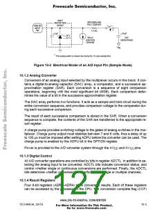
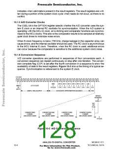
10.1.6 Conversion Sequence
A/D converter operations are performed in sequences of four conversions each. A
conversion sequence can repeat continuously or stop after one iteration. The conver-
sion complete flag (CCF) is set after the fourth conversion in a sequence to show the
availability of data in the result registers. Figure 10-3 shows the timing of a typical se-
quence. Synchronization is referenced to the system E clock.
E CLOCK
MSB
4
CYCLES
BIT 6 BIT 5 BIT 4 BIT 3 BIT 2 BIT 1 LSB
WRITE
TO
12 E CYCLES
2
2
2
2
2
2
2
2
CYC CYC CYC CYC CYC CYC CYC CYC
ADCTL
SAMPLE ANALOG INPUT
SUCCESSIVE APPROXIMATION SEQUENCE END
REPEAT
SEQUENCE
IF
SCAN = 1
SET
CCF
FLAG
CONVERT FIRST
CHANNEL
AND UPDATE ADDR1
CONVERT SECOND
CHANNEL
AND UPDATE ADDR2
CONVERT THIRD
CHANNEL
AND UPDATE ADDR3
CONVERT FOURTH
CHANNEL
AND UPDATE ADDR4
0
32
64
96
128
E
CYCLES
Figure 10-3 A/D Conversion Sequence
ANALOG-TO-DIGITAL CONVERTER
MC68HC11F1
10-4
TECHNICAL DATA
For More Information On This Product,
Go to: www.freescale.com

 FREESCALE [ Freescale ]