Freescale Semiconductor, Inc.
10.2 A/D Converter Power-Up and Clock Select
Bit 7 of the OPTION register controls A/D converter power up. Clearing ADPU re-
moves power from and disables the A/D converter system. Setting ADPU enables the
A/D converter system. Stabilization of the analog bias voltages requires a delay of as
much as 100 µs after turning on the A/D converter. When the A/D converter system is
operating with the MCU E clock, all switching and comparator operations are synchro-
nized to the MCU clocks. This allows the comparator results to be sampled at quiet
times, which minimizes noise errors. The internal RC oscillator is asynchronous to the
MCU clock, so noise affects A/D converter results, which lowers accuracy slightly
while CSEL = 1.
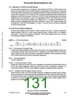
OPTION — System Configuration Options
$1039
Bit 7
ADPU
0
6
CSEL
0
5
IRQE*
0
4
DLY*
1
3
CME
0
2
FCME*
0
1
CR1*
0
Bit 0
CR0*
0
RESET:
*Can be written only once in first 64 cycles out of reset in normal modes, or at any time in special modes
ADPU — A/D Power-Up
0 = A/D powered down
1 = A/D powered up
CSEL — Clock Select
0 = A/D and EEPROM use system E clock
1 = A/D and EEPROM use internal RC clock
IRQE — Configure IRQ for Edge-Sensitive Only Operation
Refer to SECTION 5 RESETS AND INTERRUPTS.
DLY — Enable Oscillator Start-up Delay
Refer to SECTION 5 RESETS AND INTERRUPTS.
CME — Clock Monitor Enable
Refer to SECTION 5 RESETS AND INTERRUPTS.
FCME — Force Clock Monitor Enable
Refer to SECTION 5 RESETS AND INTERRUPTS.
CR[1:0] — COP Timer Rate Select Bits
Refer to SECTION 5 RESETS AND INTERRUPTS and SECTION 9 TIMING SYS-
TEM.
10.3 Conversion Process
The A/D conversion sequence begins one E-clock cycle after a write to the A/D control/
status register, ADCTL. The bits in ADCTL select the channel and the mode of con-
version.
An input voltage equal to V converts to $00 and an input voltage equal to V
con-
RL
RH
verts to $FF (full scale), with no overflow indication. For ratiometric conversions of this
type, the source of each analog input should use V
as the supply voltage and be
RH
referenced to V .
RL
ANALOG-TO-DIGITAL CONVERTER
TECHNICAL DATA
10-5
For More Information On This Product,
Go to: www.freescale.com

 FREESCALE [ Freescale ]