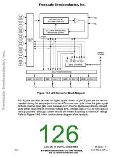
Freescale Semiconductor, Inc.
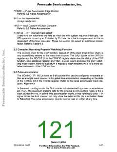
9.6.3 Pulse Accumulator Status and Interrupt Bits
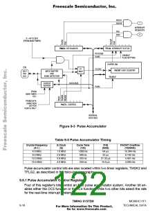
The pulse accumulator control bits, PAOVI, PAII, PAOVF, and PAIF are located within
timer registers TMSK2 and TFLG2.
TMSK2 — Timer Interrupt Mask 2 Register
$1024
Bit 7
TOI
0
6
RTII
0
5
PAOVI
0
4
PAII
0
3
—
0
2
—
0
1
PR1
0
Bit 0
PR0
0
RESET:
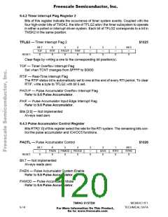
TFLG2 — Timer Interrupt Flag 2 Register
$1025
Bit 7
TOF
0
6
RTIF
0
5
PAOVF
0
4
PAIF
0
3
—
0
2
—
0
1
—
0
Bit 0
—
RESET:
0
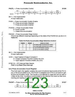
PAOVI and PAOVF — Pulse Accumulator Interrupt Enable and Overflow Flag
The PAOVF status bit is set each time the pulse accumulator count rolls over from $FF
to $00. To clear this status bit, write a one in the corresponding data bit position (bit 5)
of the TFLG2 register. The PAOVI control bit allows configuring the pulse accumulator
overflow for polled or interrupt-driven operation and does not affect the state of
PAOVF. When PAOVI is zero, pulse accumulator overflow interrupts are inhibited, and
the system operates in a polled mode, which requires that PAOVF be polled by user
software to determine when an overflow has occurred. When the PAOVI control bit is
set, a hardware interrupt request is generated each time PAOVF is set. Before leaving
the interrupt service routine, software must clear PAOVF by writing to the TFLG2 reg-
ister.
PAII and PAIF — Pulse Accumulator Input Edge Interrupt Enable and Flag
The PAIF status bit is automatically set each time a selected edge is detected at the
PA7/PAI/OC1 pin. To clear this status bit, write to the TFLG2 register with a one in the
corresponding data bit position (bit 4). The PAII control bit allows configuring the pulse
accumulator input edge detect for polled or interrupt-driven operation but does not af-
fect setting or clearing the PAIF bit. When PAII is zero, pulse accumulator input inter-
rupts are inhibited, and the system operates in a polled mode. In this mode, the PAIF
bit must be polled by user software to determine when an edge has occurred. When
the PAII control bit is set, a hardware interrupt request is generated each time PAIF is
set. Before leaving the interrupt service routine, software must clear PAIF by writing to
the TFLG2 register.
TIMING SYSTEM
MC68HC11F1
9-18
TECHNICAL DATA
For More Information On This Product,
Go to: www.freescale.com

 FREESCALE [ Freescale ]