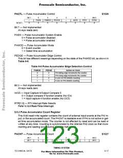
Freescale Semiconductor, Inc.
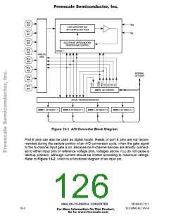
INPUT
DIFFUSION AND
PROTECTION
POLY COUPLER
DEVICE
ANALOG
INPUT
PIN
≤ 4 kΩ
*
20 pF
< 2 pF
~
+
–
20 V
0.7 V
~
~
400 nA
JUNCTION
LEAKAGE
DAC
CAPACITANCE
V
RL
*
This analog switch is closed only during the 12-cycle sample time.
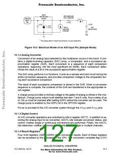
Figure 10-2 Electrical Model of an A/D Input Pin (Sample Mode)
10.1.2 Analog Converter
Conversion of an analog input selected by the multiplexer occurs in this block. It con-
tains a digital-to-analog capacitor (DAC) array, a comparator, and a successive ap-
proximation register (SAR). Each conversion is a sequence of eight comparison
operations, beginning with the most significant bit (MSB). Each comparison deter-
mines the value of a bit in the successive approximation register.
The DAC array performs two functions. It acts as a sample and hold circuit during the
entire conversion sequence, and provides comparison voltage to the comparator dur-
ing each successive comparison.
The result of each successive comparison is stored in the SAR. When a conversion
sequence is complete, the contents of the SAR are transferred to the appropriate re-
sult register.
A charge pump provides switching voltage to the gates of analog switches in the mul-
tiplexer. Charge pump output must stabilize between 7 and 8 volts, thus a delay of up
to 100 µs must be imposed after setting ADPU before the converter can be used. The
charge pump is enabled by the ADPU bit in the OPTION register.
Power is provided to the A/D converter system through the AV
and AV pins.
SS
DD
10.1.3 Digital Control
All A/D converter operations are controlled by bits in register ADCTL. In addition to se-
lecting the analog input to be converted, ADCTL bits indicate conversion status, and
control whether single or continuous conversions are performed. Finally, the ADCTL
bits determine whether conversions are performed on single or multiple channels.
10.1.4 Result Registers
Four 8-bit registers (ADR1–ADR4) store conversion results. Each of these registers
can be accessed by the processor in the CPU. The conversion complete flag (CCF)
ANALOG-TO-DIGITAL CONVERTER
TECHNICAL DATA
10-3
For More Information On This Product,
Go to: www.freescale.com

 FREESCALE [ Freescale ]