Freescale Semiconductor, Inc.
NOTE
When the multiple-channel continuous scan mode is used, extra care
is needed in the design of circuitry driving the A/D inputs. The charge
on the capacitive DAC array before the sample time is related to the
voltage on the previously converted channel. A charge share situa-
tion exists between the internal DAC capacitance and the external
circuit capacitance. Although the amount of charge involved is small,
the rate at which it is repeated is every 64 µs for an E clock of 2 MHz.
The RC charging rate of the external circuit must be balanced against
this charge sharing effect to avoid errors in accuracy. Refer to
M68HC11 Reference Manual (M68HC11RM/AD) for further informa-
tion.
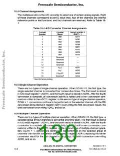
CD–CA — Channel Selects D–A
Refer to Table 10-2. When a multiple channel mode is selected (MULT = 1), the two
least significant channel select bits (CB and CA) have no meaning and the CD and CC
bits specify which group of four channels is to be converted.
Table 10-2 A/D Converter Channel Selection
Channel Select
Control Bits
Channel Signal
Result in ADRx if
MULT = 1
CD:CC:CB:CA
0000
AN0
AN1
ADR1
ADR2
ADR3
ADR4
ADR1
ADR2
ADR3
ADR4
—
0001
0010
AN2
0011
AN3
0100
AN4
0101
AN5
0110
AN6
0111
AN7
1000
Reserved
Reserved
Reserved
Reserved
1001
—
1010
—
1011
—
1100
V
RH
*
ADR1
1101
1110
1111
V
*
ADR2
ADR3
ADR4
RL
(V )/2*
RH
Reserved*
*Used for factory testing
10.9 A/D Converter Result Registers
These read-only registers hold an 8-bit conversion result. Writes to these registers
have no effect. Data in the A/D converter result registers is valid when the CCF flag in
the ADCTL register is set, indicating a conversion sequence is complete. If conversion
results are needed sooner, refer to Figure 10-3, which shows the A/D conversion se-
quence diagram.
ANALOG-TO-DIGITAL CONVERTER
MC68HC11F1
10-8
TECHNICAL DATA
For More Information On This Product,
Go to: www.freescale.com

 FREESCALE [ Freescale ]