Freescale Semiconductor, Inc.
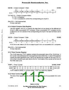
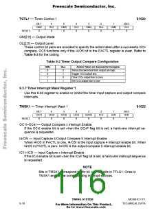
TCTL1 — Timer Control 1
$1020
Bit 7
OM2
0
6
OL2
0
5
OM3
0
4
OL3
0
3
OM4
0
2
OL4
0
1
OM5
0
Bit 0
OL5
0
RESET:
OM[2:5] — Output Mode
OL[2:5] — Output Level
These control bit pairs are encoded to specify the action taken after a successful OCx
compare. OC5 functions only if the I4/O5 bit in the PACTL register is clear. Refer to
Table 9-3 for the coding.
Table 9-2 Timer Output Compare Configuration
OMx
OLx
Action Taken on Successful Compare
Timer disconnected from output pin logic
Toggle OCx output line
0
0
1
1
0
1
0
1
Clear OCx output line to zero
Set OCx output line to one
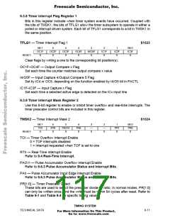
9.3.7 Timer Interrupt Mask Register 1
Use this 8-bit register to enable or inhibit the timer input capture and output compare
interrupts.
TMSK1 — Timer Interrupt Mask 1
$1022
Bit 7
OC1I
0
6
OC2I
0
5
OC3I
0
4
OC4I
0
3
I4/O5I
0
2
IC1I
0
1
IC2I
0
Bit 0
IC3I
0
RESET:
OC1I–OC4I — Output Compare x Interrupt Enable
If the OCxI enable bit is set when the OCxF flag bit is set, a hardware interrupt se-
quence is requested.
I4/O5I — Input Capture 4/Output Compare 5 Interrupt Enable
When I4/O5 in PACTL is one, I4/O5I is the input capture 4 interrupt enable bit. When
I4/O5 in PACTL is zero, I4/O5I is the output compare 5 interrupt enable bit.
IC1I–IC3I — Input Capture x Interrupt Enable
If the ICxI enable bit is set when the ICxF flag bit is set, a hardware interrupt sequence
is requested.
NOTE
Bits in TMSK1 correspond bit for bit with flag bits in TFLG1. Ones in
TMSK1 enable the corresponding interrupt sources.
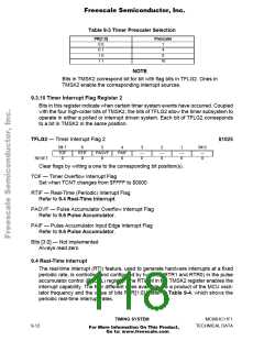
TIMING SYSTEM
MC68HC11F1
9-10
TECHNICAL DATA
For More Information On This Product,
Go to: www.freescale.com

 FREESCALE [ Freescale ]