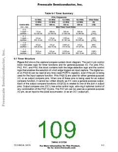
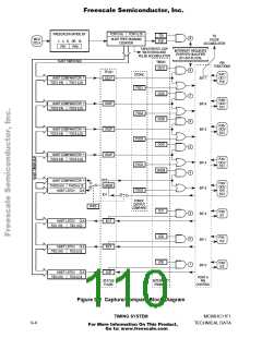
Freescale Semiconductor, Inc.
To produce a pulse of a specific duration, write a value to the output compare register
that represents the time the leading edge of the pulse is to occur. The output compare
circuit is configured to set the appropriate output either high or low, depending on the
polarity of the pulse being produced. After a match occurs, the output compare register
is reprogrammed to change the output pin back to its inactive level at the next match.
A value representing the width of the pulse is added to the original value, and then writ-
ten to the output compare register. Because the pin state changes occur at specific
values of the free-running counter, the pulse width can be controlled accurately at the
resolution of the free-running counter, independent of software latencies. To generate
an output signal of a specific frequency and duty cycle, repeat this pulse-generating
procedure.
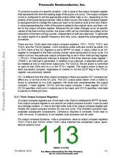
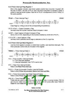
There are four 16-bit read/write output compare registers: TOC1, TOC2, TOC3, and
TOC4, and the TI4/O5 register, which functions under software control as either IC4
or OC5. Each of the OC registers is set to $FFFF on reset. A value written to an OC
register is compared to the free-running counter value during each E-clock cycle. If a
match is found, the particular output compare flag is set in timer interrupt flag register
1 (TFLG1). If that particular interrupt is enabled in the timer interrupt mask register 1
(TMSK1), an interrupt is generated. In addition to an interrupt, a specified action can
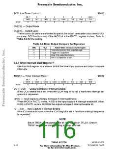
be initiated at one or more timer output pins. For OC[5:2], the pin action is controlled
by pairs of bits (OMx and OLx) in the TCTL1 register. The output action is taken on
each successful compare, regardless of whether or not the OCxF flag in the TFLG1
register was previously cleared.
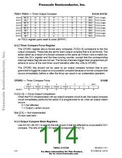
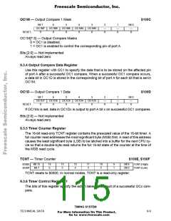
OC1 is different from the other output compares in that a successful OC1 compare can
affect any or all five of the OC pins. The OC1 output action taken when a match is
found is controlled by two 8-bit registers with three bits unimplemented: the output
compare 1 mask register, OC1M, and the output compare 1 data register, OC1D.
OC1M specifies which port A outputs are to be used, and OC1D specifies what data
is placed on these port pins.
9.3.1 Timer Output Compare Registers
All output compare registers are 16-bit read-write. Each is initialized to $FFFF at reset.
If an output compare register is not used for an output compare function, it can be used
as a storage location. A write to the high-order byte of an output compare register pair
inhibits the output compare function for one bus cycle. This inhibition prevents inap-
propriate subsequent comparisons. Coherency requires a complete 16-bit read or
write. However, if coherency is not needed, byte accesses can be used.
For output compare functions, write a comparison value to output compare registers
TOC1–TOC4 and TI4/O5. When TCNT value matches the comparison value, speci-
fied pin actions occur.
TIMING SYSTEM
TECHNICAL DATA
9-7
For More Information On This Product,
Go to: www.freescale.com

 FREESCALE [ Freescale ]