Freescale Semiconductor, Inc.
MISO/
PD2
S
INTERNAL
MCU CLOCK
M
MSB
LSB
MOSI/
PD3
M
S
8-BIT SHIFT REGISTER
READ DATA BUFFER
DIVIDER
÷2 ÷4 ÷16 ÷32
PIN
CONTROL
LOGIC
CLOCK
SPI CLOCK (MASTER)
SELECT
S
CLOCK
LOGIC
SCK/
PD4
M
S
S PR 0
SS/
PD5
MSTR
SPE
SPI CONTROL
SPIE
SPSR SPI STATUS REGISTER
SPCR SPI CONTROL REGISTER
8
8
8
SPI INTERRUPT
REQUEST
INTERNAL
DATA BUS
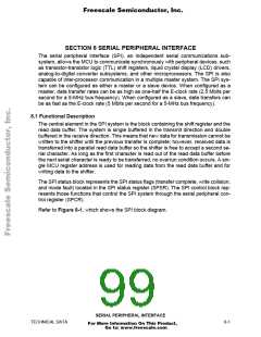
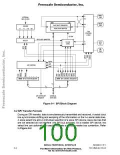
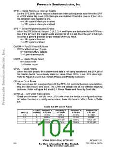
Figure 8-1 SPI Block Diagram
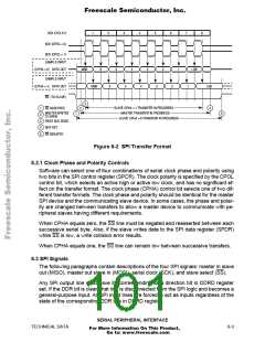
8.2 SPI Transfer Formats
During an SPI transfer, data is simultaneously transmitted and received. A serial clock
line synchronizes shifting and sampling of the information on the two serial data lines.
A slave select line allows individual selection of a slave SPI device; slave devices that
are not selected do not interfere with SPI bus activities. On a master SPI device, the
select line can optionally be used to indicate a multiple master bus contention. Refer
to Figure 8-2.
SERIAL PERIPHERAL INTERFACE
MC68HC11F1
8-2
TECHNICAL DATA
For More Information On This Product,
Go to: www.freescale.com

 FREESCALE [ Freescale ]