Freescale Semiconductor, Inc.
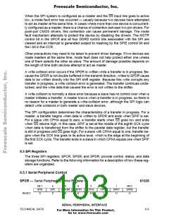
SPIE — Serial Peripheral Interrupt Enable
Set the SPE bit to one to request a hardware interrupt sequence each time the SPIF
or MODF status flag is set. SPI interrupts are inhibited if this bit is clear or if the I bit in
the condition code register is one.
0 = SPI system interrupts disabled
1 = SPI system interrupts enabled
SPE — Serial Peripheral System Enable
When the SPE bit is set, the port D bit 2, 3, 4, and 5 pins are dedicated to the SPI func-
tion. If the SPI is in the master mode and DDRD bit 5 is set, then the port D bit 5 pin
becomes a general-purpose output instead of the SS input.
0 = SPI system disabled
1 = SPI system enabled
DWOM — Port D Wired-OR Mode
DWOM affects all port D pins.
0 = Normal CMOS outputs
1 = Open-drain outputs
MSTR — Master Mode Select
0 = Slave mode
1 = Master mode
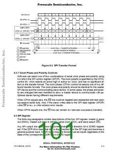
CPOL — Clock Polarity
When the clock polarity bit is cleared and data is not being transferred, the SCK pin of
the master device has a steady state low value. When CPOL is set, SCK idles high.
Refer to Figure 8-2 and 8.2.1 Clock Phase and Polarity Controls.
CPHA — Clock Phase
The clock phase bit, in conjunction with the CPOL bit, controls the clock-data relation-
ship between master and slave. The CPHA bit selects one of two different clocking
protocols. Refer to Figure 8-2 and 8.2.1 Clock Phase and Polarity Controls.
SPR[1:0] — SPI Clock Rate Selects
These two bits select the SPI clock (SCK) rate when the device is configured as mas-
ter. When the device is configured as slave, these bits have no effect. Refer to Table
8-1.
Table 8-1 SPI Clock Rates
E Clock Frequency at
Frequency at
E = 3 MHz
Frequency at
E = 4 MHz
Frequency at
E = 5 MHz
SPR[1:0]
0 0
Divide By
E = 2 MHz
1.0 MHz
500 kHz
125 kHz
62.5 kHz
2
4
1.5 MHz
750 kHz
2.0 MHz
1.0 MHz
250 kHz
125 kHz
2.5 MHz
625 kHz
0 1
1 0
16
32
187.5 kHz
93.7 kHz
156.25 kHz
78.125 kHz
1 1
SERIAL PERIPHERAL INTERFACE
MC68HC11F1
TECHNICAL DATA
8-6
For More Information On This Product,
Go to: www.freescale.com

 FREESCALE [ Freescale ]