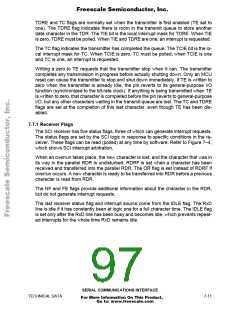
Freescale Semiconductor, Inc.
SCK CYCLE #
1
2
3
4
5
6
7
8
SCK (CPOL = 0)
SCK (CPOL = 1)
SAMPLE INPUT
(CPHA = 0) DATA OUT
MSB
6
5
4
3
2
1
LSB
SAMPLE INPUT
(CPHA = 1) DATA OUT
MSB
6
5
4
3
2
1
LSB
4
SS (TO SLAVE)
3
SLAVE CPHA = 1 TRANSFER IN PROGRESS
MASTER TRANSFER IN PROGRESS
1
2
3
4
5
2
SS ASSERTED
MASTER WRITES
TO SPDR
FIRST SCK EDGE
1
5
SLAVE CPHA = 0 TRANSFER IN PROGRESS
SPIF SET
SS NEGATED
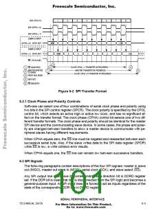
Figure 8-2 SPI Transfer Format
8.2.1 Clock Phase and Polarity Controls
Software can select one of four combinations of serial clock phase and polarity using
two bits in the SPI control register (SPCR). The clock polarity is specified by the CPOL
control bit, which selects an active high or active low clock, and has no significant ef-
fect on the transfer format. The clock phase (CPHA) control bit selects one of two dif-
ferent transfer formats. The clock phase and polarity should be identical for the master
SPI device and the communicating slave device. In some cases, the phase and polar-
ity are changed between transfers to allow a master device to communicate with pe-
ripheral slaves having different requirements.
When CPHA equals zero, the SS line must be negated and reasserted between each
successive serial byte. Also, if the slave writes data to the SPI data register (SPDR)
while SS is low, a write collision error results.
When CPHA equals one, the SS line can remain low between successive transfers.
8.3 SPI Signals
The following paragraphs contain descriptions of the four SPI signals: master in slave
out (MISO), master out slave in (MOSI), serial clock (SCK), and slave select (SS).
Any SPI output line must have its corresponding data direction bit in DDRD register
set. If the DDR bit is clear, that line is disconnected from the SPI logic and becomes a
general-purpose input. All SPI input lines are forced to act as inputs regardless of the
state of the corresponding DDR bits in DDRD register.
SERIAL PERIPHERAL INTERFACE
TECHNICAL DATA
8-3
For More Information On This Product,
Go to: www.freescale.com

 FREESCALE [ Freescale ]