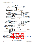
Timer Module (TIM16B8CV2) Block Description
The prescaler divides the bus clock by a prescalar value. Prescaler select bits PR[2:0] of in timer system
control register 2 (TSCR2) are set to define a prescalar value that generates a divide by 1, 2, 4, 8, 16, 32,
64 and 128 when the PRNT bit in TSCR1 is disabled.
By enabling the PRNT bit of the TSCR1 register, the performance of the timer can be enhanced. In this
case, it is possible to set additional prescaler settings for the main timer counter in the present timer by
using PTPSR[7:0] bits of PTPSR register.
14.4.2 Input Capture
Clearing the I/O (input/output) select bit, IOSx, configures channel x as an input capture channel. The
input capture function captures the time at which an external event occurs. When an active edge occurs on
the pin of an input capture channel, the timer transfers the value in the timer counter into the timer channel
registers, TCx.
The minimum pulse width for the input capture input is greater than two bus clocks.
An input capture on channel x sets the CxF flag. The CxI bit enables the CxF flag to generate interrupt
requests. Timer module or Pulse Accumulator must stay enabled (TEN bit of TSCR1 or PAEN bit of
PACTL regsiter must be set to one) while clearing CxF (writing one to CxF).
14.4.3 Output Compare
Setting the I/O select bit, IOSx, configures channel x as an output compare channel. The output compare
function can generate a periodic pulse with a programmable polarity, duration, and frequency. When the
timer counter reaches the value in the channel registers of an output compare channel, the timer can set,
clear, or toggle the channel pin if the corresponding OCPDx bit is set to zero. An output compare on
channel x sets the CxF flag. The CxI bit enables the CxF flag to generate interrupt requests. Timer module
or Pulse Accumulator must stay enabled (TEN bit of TSCR1 or PAEN bit of PACTL regsiter must be set
to one) while clearing CxF (writing one to CxF).
The output mode and level bits, OMx and OLx, select set, clear, toggle on output compare. Clearing both
OMx and OLx results in no output compare action on the output compare channel pin.
Setting a force output compare bit, FOCx, causes an output compare on channel x. A forced output
compare does not set the channel flag.
A channel 7 event, which can be a counter overflow when TTOV[7] is set or a successful output compare
on channel 7, overrides output compares on all other output compare channels. The output compare 7 mask
register masks the bits in the output compare 7 data register. The timer counter reset enable bit, TCRE,
enables channel 7 output compares to reset the timer counter. A channel 7 output compare can reset the
timer counter even if the IOC7 pin is being used as the pulse accumulator input.
Writing to the timer port bit of an output compare pin does not affect the pin state. The value written is
stored in an internal latch. When the pin becomes available for general-purpose output, the last value
written to the bit appears at the pin.
S12P-Family Reference Manual, Rev. 1.13
Freescale Semiconductor
497

 FREESCALE [ Freescale ]