Timer Module (TIM16B8CV2) Block Description
To operate the 16-bit pulse accumulator independently of input capture or output compare 7 and 0
respectively the user must set the corresponding bits IOSx = 1, OMx = 0 and OLx = 0. OC7M7 in the
OC7M register must also be cleared.
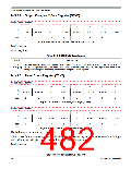
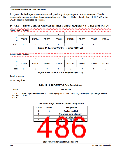
14.3.2.9 Timer Control Register 3/Timer Control Register 4 (TCTL3 and TCTL4)
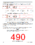
Module Base + 0x000A
7
6
5
4
3
2
1
0
R
W
EDG7B
EDG7A
EDG6B
EDG6A
EDG5B
EDG5A
EDG4B
EDG4A
Reset
0
0
0
0
0
0
0
0
Figure 14-16. Timer Control Register 3 (TCTL3)
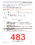
Module Base + 0x000B
7
6
5
4
3
2
1
0
R
EDG3B
W
EDG3A
EDG2B
EDG2A
EDG1B
EDG1A
EDG0B
EDG0A
Reset
0
0
0
0
0
0
0
0
Figure 14-17. Timer Control Register 4 (TCTL4)
Read: Anytime
Write: Anytime.
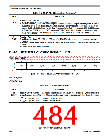
Table 14-10. TCTL3/TCTL4 Field Descriptions
Description
Field
7:0
Input Capture Edge Control — These eight pairs of control bits configure the input capture edge detector
EDGnB
EDGnA
circuits.
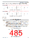
Table 14-11. Edge Detector Circuit Configuration
EDGnB
EDGnA
Configuration
0
0
1
1
0
1
0
1
Capture disabled
Capture on rising edges only
Capture on falling edges only
Capture on any edge (rising or falling)
S12P-Family Reference Manual, Rev. 1.13
486
Freescale Semiconductor

 FREESCALE [ Freescale ]