Timer Module (TIM16B8CV2) Block Description
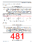
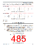
14.3.2.8 Timer Control Register 1/Timer Control Register 2 (TCTL1/TCTL2)
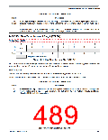
Module Base + 0x0008
7
6
5
4
3
2
1
0
R
W
OM7
OL7
OM6
OL6
OM5
OL5
OM4
OL4
Reset
0
0
0
0
0
0
0
0
Figure 14-14. Timer Control Register 1 (TCTL1)
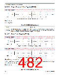
Module Base + 0x0009
7
6
5
4
3
2
1
0
R
OM3
W
OL3
OM2
OL2
OM1
OL1
OM0
OL0
Reset
0
0
0
0
0
0
0
0
Figure 14-15. Timer Control Register 2 (TCTL2)
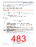
Read: Anytime
Write: Anytime
Table 14-8. TCTL1/TCTL2 Field Descriptions
Description
Field
7:0
OMx
Output Mode — These eight pairs of control bits are encoded to specify the output action to be taken as a result
of a successful OCx compare. When either OMx or OLx is 1, the pin associated with OCx becomes an output
tied to OCx.
Note: To enable output action by OMx bits on timer port, the corresponding bit in OC7M should be cleared. For
an output line to be driven by an OCx the OCPDx must be cleared.
7:0
OLx
Output Level — These eight pairs of control bits are encoded to specify the output action to be taken as a result
of a successful OCx compare. When either OMx or OLx is 1, the pin associated with OCx becomes an output
tied to OCx.
Note: To enable output action by OLx bits on timer port, the corresponding bit in OC7M should be cleared. For
an output line to be driven by an OCx the OCPDx must be cleared.
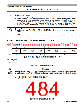
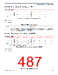
Table 14-9. Compare Result Output Action
OMx
OLx
Action
0
0
No output compare
action on the timer output signal
0
1
1
1
0
1
Toggle OCx output line
Clear OCx output line to zero
Set OCx output line to one
S12P-Family Reference Manual, Rev. 1.13
Freescale Semiconductor
485

 FREESCALE [ Freescale ]