Timer Module (TIM16B8CV2) Block Description
Read: Anytime but will always return 0x0000 (1 state is transient)
Write: Anytime
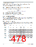
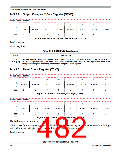
Table 14-3. CFORC Field Descriptions
Description
Field
7:0
FOC[7:0]
Force Output Compare Action for Channel 7:0 — A write to this register with the corresponding data bit(s) set
causes the action which is programmed for output compare “x” to occur immediately. The action taken is the
same as if a successful comparison had just taken place with the TCx register except the interrupt flag does not
get set.
Note: A channel 7 event, which can be a counter overflow when TTOV[7] is set or a successful output compare
on channel 7, overrides any channel 6:0 compares. If forced output compare on any channel occurs at the
same time as the successful output compare then forced output compare action will take precedence and
interrupt flag won’t get set.
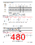
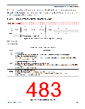
14.3.2.3 Output Compare 7 Mask Register (OC7M)
Module Base + 0x0002
7
6
5
4
3
2
1
0
R
W
OC7M7
OC7M6
OC7M5
OC7M4
OC7M3
OC7M2
OC7M1
OC7M0
Reset
0
0
0
0
0
0
0
0
Figure 14-8. Output Compare 7 Mask Register (OC7M)
Read: Anytime
Write: Anytime
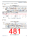
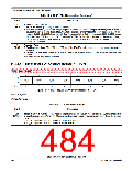
Table 14-4. OC7M Field Descriptions
Description
Field
7:0
Output Compare 7 Mask — A channel 7 event, which can be a counter overflow when TTOV[7] is set or a
OC7M[7:0] successful output compare on channel 7, overrides any channel 6:0 compares. For each OC7M bit that is set,
the output compare action reflects the corresponding OC7D bit.
0 The corresponding OC7Dx bit in the output compare 7 data register will not be transferred to the timer port on
a channel 7 event, even if the corresponding pin is setup for output compare.
1 The corresponding OC7Dx bit in the output compare 7 data register will be transferred to the timer port on a
channel 7 event.
Note: The corresponding channel must also be setup for output compare (IOSx = 1 and OCPDx = 0) for data to
be transferred from the output compare 7 data register to the timer port.
S12P-Family Reference Manual, Rev. 1.13
Freescale Semiconductor
481

 FREESCALE [ Freescale ]