Timer Module (TIM16B8CV2) Block Description
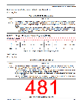
14.2.7 IOC1 — Input Capture and Output Compare Channel 1 Pin
This pin serves as input capture or output compare for channel 1.
14.2.8 IOC0 — Input Capture and Output Compare Channel 0 Pin
This pin serves as input capture or output compare for channel 0.
NOTE
For the description of interrupts see Section 14.6, “Interrupts”.
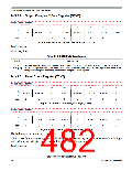
14.3 Memory Map and Register Definition
This section provides a detailed description of all memory and registers.
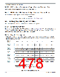
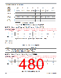
14.3.1 Module Memory Map
The memory map for the TIM16B8CV2 module is given below in Figure 14-5. The address listed for each
register is the address offset. The total address for each register is the sum of the base address for the
TIM16B8CV2 module and the address offset for each register.
14.3.2 Register Descriptions
This section consists of register descriptions in address order. Each description includes a standard
register diagram with an associated figure number. Details of register bit and field function follow the
register diagrams, in bit order.
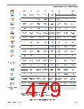
Register
Name
Bit 7
6
5
4
3
2
1
Bit 0
0x0000
TIOS
R
IOS7
IOS6
IOS5
IOS4
IOS3
IOS2
IOS1
IOS0
W
0x0001
CFORC
R
0
0
0
0
0
0
0
0
W
FOC7
FOC6
FOC5
FOC4
FOC3
FOC2
FOC1
FOC0
0x0002
OC7M
R
OC7M7
OC7D7
TCNT15
TCNT7
OC7M6
OC7D6
TCNT14
TCNT6
OC7M5
OC7D5
TCNT13
TCNT5
OC7M4
OC7D4
TCNT12
TCNT4
OC7M3
OC7D3
TCNT11
TCNT3
OC7M2
OC7D2
TCNT10
TCNT2
OC7M1
OC7D1
TCNT9
TCNT1
OC7M0
OC7D0
TCNT8
TCNT0
W
0x0003
OC7D
R
W
0x0004
TCNTH
R
W
0x0005
TCNTL
R
W
= Unimplemented or Reserved
Figure 14-5. TIM16B8CV2 Register Summary (Sheet 1 of 3)
S12P-Family Reference Manual, Rev. 1.13
478
Freescale Semiconductor

 FREESCALE [ Freescale ]