Timer Module (TIM16B8CV2) Block Description
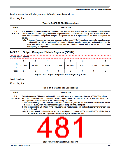
Register
Bit 7
6
5
4
3
2
1
Bit 0
Name
0x002C
OCPD
R
OCPD7
OCPD6
OCPD5
OCPD4
OCPD3
OCPD2
OCPD1
OCPD0
W
0x002D
R
0x002E
PTPSR
R
PTPS7
PTPS6
PTPS5
PTPS4
PTPS3
PTPS2
PTPS1
PTPS0
W
0x002F
R
Reserved
W
= Unimplemented or Reserved
Figure 14-5. TIM16B8CV2 Register Summary (Sheet 3 of 3)
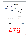
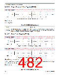
14.3.2.1 Timer Input Capture/Output Compare Select (TIOS)
Module Base + 0x0000
7
6
5
4
3
2
1
0
R
W
IOS7
IOS6
IOS5
IOS4
IOS3
IOS2
IOS1
IOS0
Reset
0
0
0
0
0
0
0
0
Figure 14-6. Timer Input Capture/Output Compare Select (TIOS)
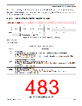
Read: Anytime
Write: Anytime
Table 14-2. TIOS Field Descriptions
Description
Field
7:0
IOS[7:0]
Input Capture or Output Compare Channel Configuration
0 The corresponding channel acts as an input capture.
1 The corresponding channel acts as an output compare.
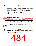
14.3.2.2 Timer Compare Force Register (CFORC)
Module Base + 0x0001
7
6
5
4
3
2
1
0
R
W
0
0
0
0
0
0
0
0
FOC7
0
FOC6
0
FOC5
0
FOC4
0
FOC3
0
FOC2
0
FOC1
0
FOC0
0
Reset
Figure 14-7. Timer Compare Force Register (CFORC)
S12P-Family Reference Manual, Rev. 1.13
480
Freescale Semiconductor

 FREESCALE [ Freescale ]