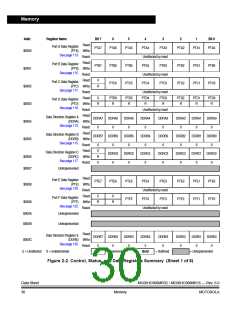
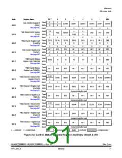
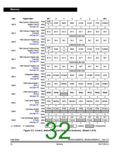
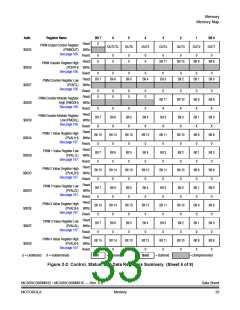
Memory
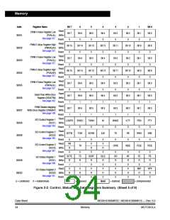
Addr.
Register Name
Bit 7
Bit 7
0
6
Bit 6
0
5
Bit 5
0
4
Bit 4
0
3
Bit 3
0
2
Bit 2
0
1
Bit 1
0
Bit 0
Bit 0
0
Read:
PWM 4 Value Register Low
$0031
(PVAL4L) Write:
See page 157.
Reset:
Read:
PWM 5 Value Register High
Bit 15
0
Bit 14
0
Bit 13
0
Bit 12
0
Bit 11
0
Bit 10
0
Bit 9
0
Bit 8
0
$0032
$0033
$0034
$0035
$0036
$0037
$0038
$0039
$003A
$003B
(PMVAL5H) Write:
See page 157.
Reset:
Read:
PWM 5 Value Register Low
Bit 7
0
Bit 6
0
Bit 5
0
Bit 4
0
Bit 3
0
Bit 2
0
Bit 1
0
Bit 0
0
(PVAL5L) Write:
See page 157.
Reset:
Read:
PWM 6 Value Register High
Bit 15
0
Bit 14
0
Bit 13
0
Bit 12
0
Bit 11
0
Bit 10
0
Bit 9
0
Bit 8
0
(PVAL6H) Write:
See page 157.
Reset:
Read:
PWM 6 Value Register Low
Bit 7
0
Bit 6
0
Bit 5
0
Bit 4
0
Bit 3
0
Bit 2
0
Bit 1
0
Bit 0
0
(PMVAL6L) Write:
See page 157.
Reset:
Read:
Dead-Time Write-Once
Register (DEADTM) Write:
Bit 7
1
Bit 6
1
Bit 5
1
Bit 4
1
Bit 3
1
Bit 2
1
Bit 1
1
Bit 0
1
See page 162.
Reset:
Read:
PWM Disable Mapping
Write-Once Register (DISMAP) Write:
Bit 7
1
Bit 6
1
Bit 5
1
Bit 4
1
Bit 3
1
Bit 2
1
Bit 1
1
Bit 0
1
See page 149.
Reset:
Read:
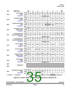
SCI Control Register 1
LOOPS
0
ENSCI
0
TXINV
0
M
WAKE
0
ILTY
0
PEN
0
PTY
0
(SCC1) Write:
See page 183.
Reset:
0
Read:
SCI Control Register 2
SCTIE
TCIE
0
SCRIE
ILIE
TE
RE
0
RWU
0
SBK
0
(SCC2) Write:
See page 185.
Reset:
0
R8
R
0
0
0
0
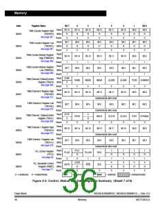
Read:
0
SCI Control Register 3
T8
ORIE
NEIE
FEIE
PEIE
(SCC3) Write:
See page 187.
Reset:
R
R
U
U
0
0
0
0
NF
R
0
0
FE
R
0
PE
R
Read: SCTE
TC
SCRF
IDLE
R
OR
SCI Status Register 1
See page 188.
(SCS1) Write:
R
1
R
R
0
R
Reset:
Read:
1
0
0
0
0
0
0
0
0
0
0
BKF
R
RPF
R
SCI Status Register 2
$003C
(SCS2) Write:
See page 191.
R
0
R
R
0
R
R
0
R
0
Reset:
0
0
0
0
U = Unaffected X = Indeterminate
R
= Reserved
Bold
= Buffered
= Unimplemented
Figure 2-2. Control, Status, and Data Registers Summary (Sheet 5 of 8)
Data Sheet
34
MC68HC908MR32 • MC68HC908MR16 — Rev. 6.0
MOTOROLA
Memory

 FREESCALE [ Freescale ]