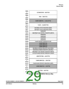
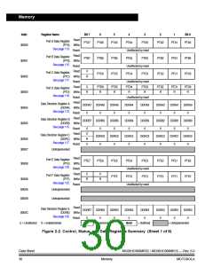
Memory
Addr.
Register Name
Bit 7
6
5
4
3
2
1
Bit 0
Read:
(PTA) Write:
Port A Data Register
PTA7
PTA6
PTA5
PTA4
PTA3
PTA2
PTA1
PTA0
$0000
See page 113.
Reset:
Read:
Unaffected by reset
PTB4 PTB3
Unaffected by reset
PTC4 PTC3
Unaffected by reset
Port B Data Register
PTB7
PTB6
PTC6
PTB5
PTC5
PTB2
PTC2
PTB1
PTC1
PTB0
PTC0
$0001
$0002
$0003
$0004
$0005
(PTB) Write:
See page 115.
Reset:
Read:
0
Port C Data Register
(PTC) Write:
R
See page 117.
Reset:
Read:
0
PTD6
R
PTD5
R
PTD4
R
PTD3
R
PTD2
R
PTD1
R
PTD0
R
Port D Data Register
(PTD) Write:
R
See page 119.
Reset:
Read:
Unaffected by reset
Data Direction Register A
DDRA7 DDRA6
DDRA5
DDRA4
DDRA3
DDRA2
DDRA1 DDRA0
(DDRA) Write:
See page 113.
Reset:
Read:
0
0
0
DDRB5
0
0
DDRB4
0
0
DDRB3
0
0
DDRB2
0
0
0
Data Direction Register B
DDRB7 DDRB6
DDRB1 DDRB0
(DDRB) Write:
See page 115.
Reset:
Read:
0
0
0
DDRC6
0
0
0
Data Direction Register C
DDRC5
0
DDRC4
0
DDRC3
0
DDRC2
0
DDRC1 DDRC0
$0006
$0007
(DDRC) Write:
R
0
See page 117.
Reset:
0
0
Unimplemented
Read:
Port E Data Register
PTE7
PTE6
PTE5
PTF5
PTE4
PTE3
PTE2
PTF2
PTE1
PTF1
PTE0
PTF0
$0008
$0009
(PTE) Write:
See page 120.
Reset:
Read:
Unaffected by reset
PTF4 PTF3
Unaffected by reset
0
0
Port F Data Register
(PTF) Write:
R
R
See page 122.
Reset:
$000A
$000B
Unimplemented
Unimplemented
Read:
Data Direction Register E
DDRE7 DDRE6
DDRE5
0
DDRE4
DDRE3
DDRE2
0
DDRE1 DDRE0
$000C
(DDRE) Write:
See page 120.
Reset:
0
0
0
0
0
0
U = Unaffected X = Indeterminate
R
= Reserved
Bold
= Buffered
= Unimplemented
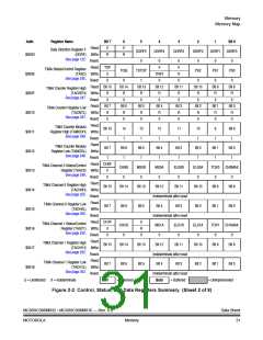
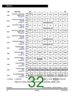
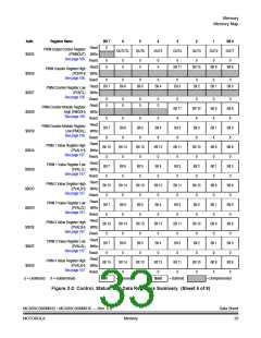
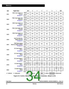
Figure 2-2. Control, Status, and Data Registers Summary (Sheet 1 of 8)
Data Sheet
30
MC68HC908MR32 • MC68HC908MR16 — Rev. 6.0
MOTOROLA
Memory

 FREESCALE [ Freescale ]