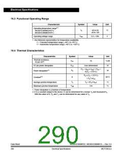
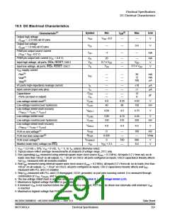
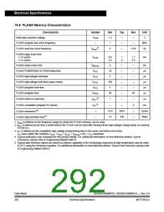
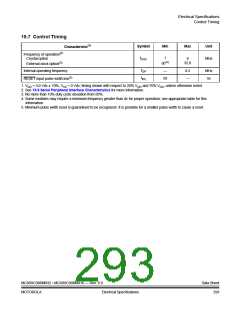
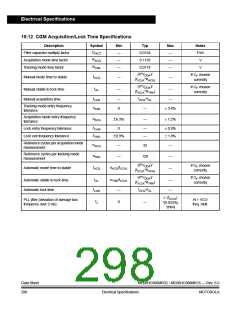
Electrical Specifications
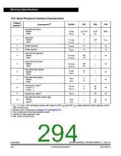
19.8 Serial Peripheral Interface Characteristics
Diagram
Characteristic(2)
Number(1)
Symbol
Min
Max
Unit
Operating frequency
Master
Slave
fOP(M)
fOP(S)
f
OP/2
f
OP/128
dc
MHz
f
OP
Cycle time
Master
Slave
tCYC(M)
tCYC(S)
tCYC
1
2
1
128
—
tLead(S)
tLag(S)
2
3
Enable lead time
Enable lag time
15
15
—
—
ns
ns
Clock (SPCK) high time
Master
Slave
tSCKH(M)
tSCKH(S)
4
5
100
50
—
—
ns
ns
Clock (SPCK) low time
Master
Slave
tSCKL(M)
tSCKL(S)
100
50
—
—
Data setup time (inputs)
Master
Slave
tSU(M)
tSU(S)
45
5
—
—
6
7
ns
ns
Data hold time (inputs)
Master
Slave
tH(M)
tH(S)
0
15
—
—
Access time, slave(3)
CPHA = 0
CHPA = 1
tA(CP0)
tA(CP1)
0
0
40
20
8
9
ns
ns
ns
Disable time, slave(4)
tDIS(S)
—
25
Data valid time after enable edge
Master
Slave(5)
tV(M)
tV(S)
10
—
—
10
40
1. VDD = 5.0 Vdc ± 10%, all timing is shown with respect to 20% VDD and 70% VDD, unless otherwise noted; assumes 100 pF
load on all SPI pins
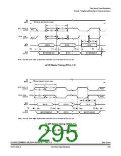
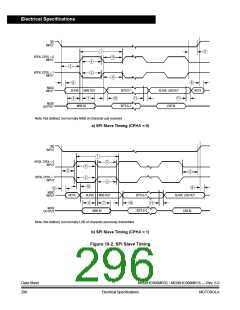
2. Numbers refer to dimensions in Figure 19-1 and Figure 19-2.
3. Time to data active from high-impedance state
4. Hold time to high-impedance state
5. With 100 pF on all SPI pins
Data Sheet
294
MC68HC908MR32 • MC68HC908MR16 — Rev. 6.0
MOTOROLA
Electrical Specifications

 FREESCALE [ Freescale ]