Electrical Specifications
TImer Interface Module Characteristics
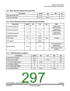
19.9 TImer Interface Module Characteristics
Characteristic
Input capture pulse width
Symbol
tTIH, TIL
TCH, tTCL
Min
125
Max
—
Unit
ns
t
t
(1/fOP) + 5
Input clock pulse width
—
ns
19.10 Clock Generation Module Component Specifications
Characteristic
Symbol
Min
Typ
Max
Notes
Consult crystal
manufacturing data
CL
Crystal load capacitance
—
—
—
Consult crystal
manufacturing data
C1
C2
2 * CL
2 * CL
Crystal fixed capacitance
Crystal tuning capacitance
—
—
—
—
Consult crystal
manufacturing data
RB
RS
Feedback bias resistor
Series resistor
—
0
22 MΩ
330 kΩ
—
1 MΩ
Not required
CFACT
*
CF
Filter capacitor
—
—
(VDDA/fXCLK
)
CBYP must provide low ac
impedance from
CBYP
Bypass capacitor
—
0.1 µF
—
f = fXCLK/100 to 100*fVCLK, so
series resistance must be
considered
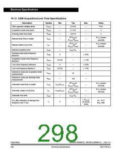
19.11 CGM Operating Conditions
Characteristic
Crystal reference frequency
Range nominal multiplier
Symbol
Min
1
Typ
Max
8
Unit
MHz
MHz
fXCLK
—
fNOM
fVRS
—
4.9152
—
VCO center-of-range frequency
VCO frequency multiplier
4.9152
—
—
—
—
32.8
15
MHz
—
N
L
1
1
VCO center of range multiplier
VCO operating frequency
15
—
fVCLK
fVRSMIN
fVRSMAX
—
MC68HC908MR32 • MC68HC908MR16 — Rev. 6.0
MOTOROLA
Data Sheet
297
Electrical Specifications

 FREESCALE [ Freescale ]