Electrical Specifications
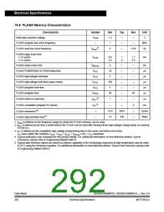
19.6 FLASH Memory Characteristics
Characteristic
RAM data retention voltage
Symbol
Min
1.3
1
Typ
—
Max
—
Unit
V
VRDR
FLASH program bus clock frequency
FLASH read bus clock frequency
—
—
—
MHz
Hz
(1)
0
—
8 M
fRead
FLASH page erase time
<1 K cycles
>1 K cycles
tErase
0.9
3.6
1
4
1.1
5.5
ms
tMErase
tNVS
FLASH mass erase time
4
10
5
—
—
—
—
—
—
—
—
—
—
—
—
40
—
ms
µs
µs
µs
µs
µs
µs
FLASH PGM/ERASE to HVEN setup time
FLASH high-voltage hold time
FLASH high-voltage hold time (mass erase)
FLASH program hold time
tNVH
tNVHL
tPGS
100
5
tPROG
FLASH program time
30
1
(2)
FLASH return to read time
tRCV
(3)
FLASH cumulative program HV period
—
10 k
15
—
4
ms
tHV
FLASH endurance(4)
—
—
100 k
100
—
—
Cycles
Years
FLASH data retention time(5)
1. fRead is defined as the frequency range for which the FLASH memory can be read.
2. tRCV is defined as the time it needs before the FLASH can be read after turning off the high voltage charge pump, by clearing
HVEN to 0.
3. tHV is defined as the cumulative high voltage programming time to the same row before next erase.
tHV must satisfy this condition: tNVS + tNVH + tPGS + (tPROG x 32) ≤ tHV maximum.
4. Typical endurance was evaluated for this product family. For additional information on how Motorola defines Typical
Endurance, please refer to Engineering Bulletin EB619.
5. Typical data retention values are based on intrinsic capability of the technology measured at high temperature and de-rated
to 25°C using the Arrhenius equation. For additional information on how Motorola defines Typical Data Retention, please refer
to Engineering Bulletin EB618.
Data Sheet
292
MC68HC908MR32 • MC68HC908MR16 — Rev. 6.0
MOTOROLA
Electrical Specifications

 FREESCALE [ Freescale ]