Electrical Specifications
DC Electrical Characteristics
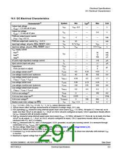
19.5 DC Electrical Characteristics
Characteristic(1)
Typ(2)
Symbol
Min
Max
Unit
Output high voltage
(ILoad = –2.0 mA) all I/O pins
VOH
VDD –0.8
—
—
V
Output low voltage
(ILoad = 1.6 mA) all I/O pins
VOL
IOH
—
—
—
0.4
—
V
PWM pin output source current
(VOH = VDD –0.8 V)
–7
mA
PWM pin output sink current (VOL = 0.8 V)
IOL
VIH
VIL
20
0.7 x VDD
VSS
—
—
—
—
mA
V
VDD
Input high voltage, all ports, IRQs, RESET, OSC1
Input low voltage, all ports, IRQs, RESET, OSC1
VDD supply current
0.3 x VDD
V
Run(3)
Wait(4)
Stop(5)
—
—
—
—
—
—
30
12
700
mA
mA
µA
IDD
IIL
IIn
I/O ports high-impedance leakage current
Input current (input only pins)
—
—
—
—
±10
±1
µA
µA
COut
CIn
Capacitance
Ports (as input or output)
—
—
—
—
12
8
pF
Low-voltage inhibit reset(6)
VLVR1
VLVH1
4.0
40
4.35
90
4.65
150
V
Low-voltage reset/recover hysteresis
mV
Low-voltage inhibit reset recovery
VREC1
4.04
4.5
4.75
V
(VREC1 = VLVR1 + VLVH1
)
VLVR2
VLVH2
Low-voltage inhibit reset
3.85
150
4.15
210
4.45
250
V
Low-voltage reset/recover hysteresis
Low-voltage inhibit reset recovery
(VREC2 = VLVR2 + VLVH2
mV
VREC2
4.0
4.4
4.6
V
)
POR re-arm voltage(7)
POR rise time ramp rate(8)
POR reset voltage(9)
VPOR
RPOR
0
0.035
0
—
—
100
—
mV
V/ms
V
VPORRST
VHi
700
—
800
8.0
VDD + 2.5
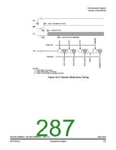
Monitor mode entry voltage (on IRQ)
V
1. VDD = 5.0 Vdc ± 10%, VSS = 0 Vdc, TA = TL to TH, unless otherwise noted.
2. Typical values reflect average measurements at midpoint of voltage range, 25°C only.
3. Run (operating) IDD measured using external square wave clock source (fOSC = 8.2 MHz). All inputs 0.2 V from rail; no dc
loads; less than 100 pF on all outputs. CL = 20 pF on OSC2; all ports configured as inputs; OSC2 capacitance linearly affects
run IDD; measured with all modules enabled
4. Wait IDD measured using external square wave clock source (fOSC = 8.2 MHz); all inputs 0.2 V from rail; no dc loads; less than
100 pF on all outputs. CL = 20 pF on OSC2; all ports configured as inputs; OSC2 capacitance linearly affects wait IDD
measured with PLL and LVI enabled.
;
5. Stop IDD measured with PLL and LVI disengaged, OCS1 grounded, no port pins sourcing current. It is measured through
combination of VDD, VDDAD, and VDDA
.
6. The low-voltage inhibit reset is software selectable. Refer to Section 9. Low-Voltage Inhibit (LVI).
7. Maximum is highest voltage that POR is guaranteed.
8. If minimum VDD is not reached before the internal POR is released, RST must be driven low externally until minimum VDD
is reached.
9. Maximum is highest voltage that POR is possible.
MC68HC908MR32 • MC68HC908MR16 — Rev. 6.0
MOTOROLA
Data Sheet
291
Electrical Specifications

 FREESCALE [ Freescale ]