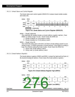
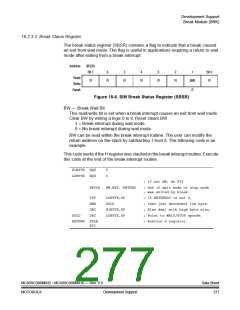
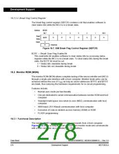
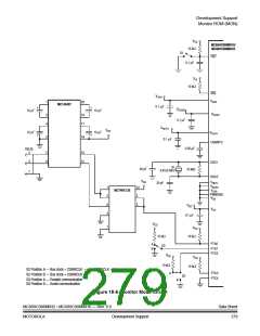
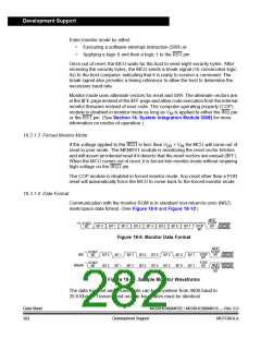
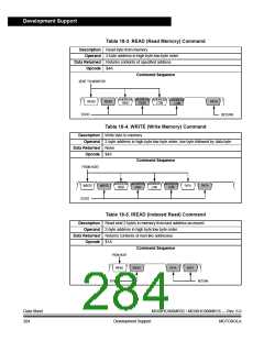
Development Support
Simple monitor commands can access any memory address. In monitor mode, the
MCU can execute host-computer code in RAM while all MCU pins retain normal
operating mode functions. All communication between the host computer and the
MCU is through the PTA0 pin. A level-shifting and multiplexing interface is required
between PTA0 and the host computer. PTA0 is used in a wired-OR configuration
and requires a pullup resistor.
18.3.1.1 Entering Monitor Mode
There are two methods for entering monitor:
•
The first is the traditional M68HC08 method where VDD + VHI is applied to
IRQ1 and the mode pins are configured appropriately.
•
A second method, intended for in-circuit programming applications, will
force entry into monitor mode without requiring high voltage on the IRQ1 pin
when the reset vector locations of the FLASH are erased ($FF).
NOTE:
For both methods, holding the PTC2 pin low when entering monitor mode causes
a bypass of a divide-by-two stage at the oscillator. The CGMOUT frequency is
equal to the CGMXCLK frequency, and the OSC1 input directly generates internal
bus clocks. In this case, the OSC1 signal must have a 50 percent duty cycle at
maximum bus frequency.
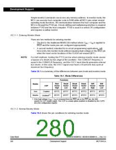
Table 18-1 is a summary of the differences between user mode and monitor mode.
Table 18-1. Mode Differences
Functions
Rest
Vector
High
Reset
Vector
Low
Break
Vector
High
Break
Vector
Low
SWI
Vector
High
SWI
Vector
Low
Modes
COP
User
Enabled
$FFFE
$FEFE
$FFFF
$FEFF
$FFFC
$FEFC
$FFFD
$FEFD
$FFFC
$FEFC
$FFFD
$FEFD
Disabled(1)
Monitor
1. If the high voltage (VDD + VHI) is removed from the IRQ1 pin or the RST pin, the SIM
asserts its COP enable output. The COP is a mask option enabled or disabled by the COPD
bit in the configuration register.
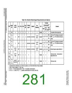
18.3.1.2 Normal Monitor Mode
Table 18-2 shows the pin conditions for entering monitor mode.
Data Sheet
280
MC68HC908MR32 • MC68HC908MR16 — Rev. 6.0
MOTOROLA
Development Support

 FREESCALE [ Freescale ]