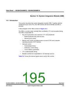
System Integration Module (SIM)
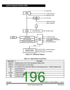
SIM Bus Clock Control and Generation
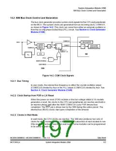
14.2 SIM Bus Clock Control and Generation
The bus clock generator provides system clock signals for the CPU and peripherals
on the MCU. The system clocks are generated from an incoming clock, CGMOUT,
as shown in Figure 14-2. This clock can come from either an external oscillator or
from the on-chip phase-locked loop (PLL) circuit. See Section 4. Clock Generator
Module (CGM).
CGMXCLK
OSC1
SIM COUNTER
CLOCK
SELECT
CIRCUIT
A
B
CGMOUT
BUS CLOCK
GENERATORS
÷ 2
÷ 2
CGMVCLK
S*
*When S = 1,
CGMOUT = B
BCS
SIM
PLL
PTC2
MONITOR MODE
USER MODE
CGM
Figure 14-2. CGM Clock Signals
14.2.1 Bus Timing
In user mode, the internal bus frequency is either the crystal oscillator output
(CGMXCLK) divided by four or the PLL output (CGMVCLK) divided by four. See
Section 4. Clock Generator Module (CGM).
14.2.2 Clock Startup from POR or LVI Reset
When the power-on reset (POR) module or the low-voltage inhibit (LVI) module
generates a reset, the clocks to the CPU and peripherals are inactive and held in
an inactive phase until after the 4096 CGMXCLK cycle POR timeout has
completed. The RST pin is driven low by the SIM during this entire period. The
internal bus (IBUS) clocks start upon completion of the timeout.
14.2.3 Clocks in Wait Mode
In wait mode, the CPU clocks are inactive. The SIM also produces two sets of
clocks for other modules. Refer to the wait mode subsection of each module to see
if the module is active or inactive in wait mode. Some modules can be programmed
to be active in wait mode.
MC68HC908MR32 • MC68HC908MR16 — Rev. 6.0
MOTOROLA System Integration Module (SIM)
Data Sheet
197

 FREESCALE [ Freescale ]