Serial Communications Interface Module (SCI)
I/O Registers
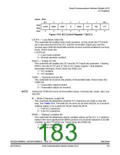
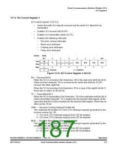
Address: $0038
Bit 7
6
ENSCI
0
5
TXINV
0
4
M
0
3
WAKE
0
2
ILTY
0
1
PEN
0
Bit 0
PTY
0
Read:
Write:
Reset:
LOOPS
0
Figure 13-8. SCI Control Register 1 (SCC1)
LOOPS — Loop Mode Select Bit
This read/write bit enables loop mode operation. In loop mode the PTF4/RxD
pin is disconnected from the SCI, and the transmitter output goes into the
receiver input. Both the transmitter and the receiver must be enabled to use loop
mode. Reset clears the
LOOPS bit.
1 = Loop mode enabled
0 = Normal operation enabled
ENSCI — Enable SCI Bit
This read/write bit enables the SCI and the SCI baud rate generator. Clearing
ENSCI sets the SCTE and TC bits in SCI status register 1 and disables
transmitter interrupts. Reset clears the ENSCI bit.
1 = SCI enabled
0 = SCI disabled
TXINV — Transmit Inversion Bit
This read/write bit reverses the polarity of transmitted data. Reset clears the
TXINV bit.
1 = Transmitter output inverted
0 = Transmitter output not inverted
NOTE:
Setting the TXINV bit inverts all transmitted values, including idle, break, start, and
stop bits.
M — Mode (Character Length) Bit
This read/write bit determines whether SCI characters are eight or nine bits
long. See Table 13-4. The ninth bit can serve as an extra stop bit, as a receiver
wakeup signal, or as a parity bit. Reset clears the M bit.
1 = 9-bit SCI characters
0 = 8-bit SCI characters
WAKE — Wakeup Condition Bit
This read/write bit determines which condition wakes up the SCI: a 1 (address
mark) in the most significant bit (MSB) position of a received character or an idle
condition on the PTF4/RxD pin. Reset clears the WAKE bit.
1 = Address mark wakeup
0 = Idle line wakeup
MC68HC908MR32 • MC68HC908MR16 — Rev. 6.0
MOTOROLA Serial Communications Interface Module (SCI)
Data Sheet
183

 FREESCALE [ Freescale ]