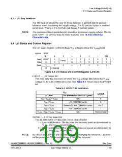
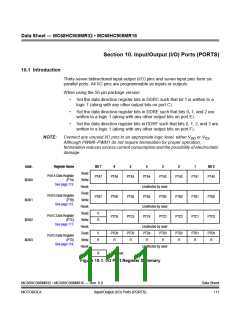
Input/Output (I/O) Ports (PORTS)
Port A
10.2 Port A
Port A is an 8-bit, general-purpose, bidirectional I/O port.
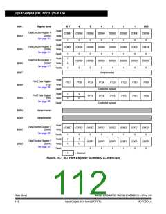
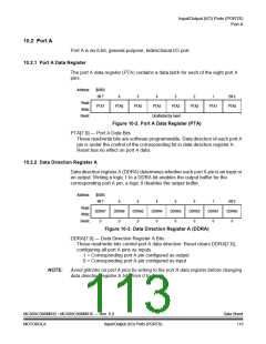
10.2.1 Port A Data Register
The port A data register (PTA) contains a data latch for each of the eight port A
pins.
Address:
$0000
Bit 7
6
5
4
3
2
1
Bit 0
Read:
Write:
Reset:
PTA7
PTA6
PTA5
PTA4
PTA3
PTA2
PTA1
PTA0
Unaffected by reset
Figure 10-2. Port A Data Register (PTA)
PTA[7:0] — Port A Data Bits
These read/write bits are software programmable. Data direction of each port A
pin is under the control of the corresponding bit in data direction register A.
Reset has no effect on port A data.
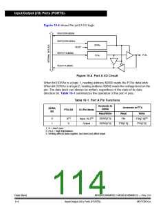
10.2.2 Data Direction Register A
Data direction register A (DDRA) determines whether each port A pin is an input or
an output. Writing a logic 1 to a DDRA bit enables the output buffer for the
corresponding port A pin; a logic 0 disables the output buffer.
Address:
$0004
Bit 7
6
DDRA6
0
5
DDRA5
0
4
DDRA4
0
3
DDRA3
0
2
DDRA2
0
1
DDRA1
0
Bit 0
DDRA0
0
Read:
Write:
Reset:
DDRA7
0
Figure 10-3. Data Direction Register A (DDRA)
DDRA[7:0] — Data Direction Register A Bits
These read/write bits control port A data direction. Reset clears DDRA[7:0],
configuring all port A pins as inputs.
1 = Corresponding port A pin configured as output
0 = Corresponding port A pin configured as input
NOTE:
Avoid glitches on port A pins by writing to the port A data register before changing
data direction register A bits from 0 to 1.
MC68HC908MR32 • MC68HC908MR16 — Rev. 6.0
MOTOROLA Input/Output (I/O) Ports (PORTS)
Data Sheet
113

 FREESCALE [ Freescale ]